Свяжитесь с компанией DONGHE

Updated June 2026 Reviewed by the Shanghai Donghe Science and Technology Co., Ltd. technical team
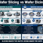
The phrase wafer slicing vs wafer dicing sounds like a choice between two rival cutting methods. It’s not. Wafer slicing vs wafer dicing is really a question about two sequential production stages, not two competing tools. Slicing and dicing are two different jobs done at opposite ends of a wafer’s life: slicing turns a crystalline ingot into bare wafers at the very start, and dicing cuts a finished, circuit-bearing wafer into individual dies at the very end. Confusing the two leads buyers to compare machines that were never alternatives, and to ignore where their real material and cost losses happen.
Short answer: (front-end) wafer slicing turns a crystalline traditional inyog (or SiC/sapphire) into a thin wafer using a алмазная проволочная пила. (back-end) wafer dicing turns a finished (completes the product life cycle) wafer into hundreds of dies by singulation using a laser, plasma, or stealth process die-saw or blade saw (dicing saw) or dicing technique (for example a stealth process). They’re stages that run one after the other on a single piece of material, in that order, not choices between one or the other.
Ключевые выводы
- Slicing is front end ( in yasou, or Asaris, or in you); dicing is back end (of a wafer in you). Different machines. Different focal points.
- Stealth dicing can leave 60µm silicon dies at 153 kgf fracture strength – the highest of any die singulation method tested.
- Blade dicing kerf runs ~20-50m; laser drops below 10m; plasma and stealth approaches zero kerf.
- In slicing, dropping diamond-wire kerf from 0.15mm to 0.06mm increases number of wafers per 200mm ingot from ~571 to ~769 (+35%).
- laser doesn’t “simply beat” blade – in fact, blade remains more cost effective even on silicon where its mount is relatively expensive and cost-driven, its sidewall quality excellent.
Quick Specs: Slicing vs Dicing
| Wafer slicing | Ingot/boule → thin bare wafers (front-end) |
| Wafer dicing | Finished wafer → individual dies (back-end / die singulation) |
| Slicing tool | Алмазная многопроводная пила |
| Dicing tools | Dicing saw, laser, plasma, stealth laser |
| Cut-width term | Slicing: wire kerf | Dicing: kerf within the street |
| Typical materials | Si, SiC, sapphire, GaN, glass |
Slicing vs Dicing at a Glance

If you only remember one thing, remember the order. A wafer is sliced once, near the beginning of its life, and diced once, near the end. In between it’s lapped, polished, doped, patterned with circuits, and often thinned. So when someone asks whether slicing or dicing is “better,” the honest answer is that the question mixes up two stages that never compete for the same job.
We suggest calling this The Slice-Then-Dice Timeline because an ingot is sliced once in the front stage, then many finished wafers are diced once in the back stage, and university fab guides describe the same front-to-back sequence, while we would like to make any process or equipment you research “fit” onto the relevant half of The 9-Point Slice-vs-Dice Matrix, below.
| Категория | Нарезка пластины | Wafer Dicing |
|---|---|---|
| Этап | Front-end (first cut) | Back-end (last cut before packaging) |
| Input | Crystalline ingot / boule | Finished, patterned wafer |
| Вывод | Bare wafers (no circuits yet) | Individual dies / chips |
| Cut-width term | Wire kerf | Kerf within the street/scribe line |
| Primary tooling | Алмазная многопроводная пила | Dicing saw, laser, plasma, stealth |
| Typical cut count | Hundreds of parallel wires at once | Thousands of streets in X and Y |
| Yield unit | Wafers per ingot | Good dies per wafer |
| Main cost driver | Kerf loss of feedstock silicon | Throughput & die-edge yield |
| Typical quality metric | Kerf, TTV, bow/warp (µm) | Chip-out size & die break strength |
Free synthesis derived from academic peer reviewed and standards sources (listed below); number of cuts per product depends on wafer diameter and die size.
Wafer Slicing, Explained: Ingot to Wafer

Wafer slicing is the front-end process that turns a grown crystalline ingot into thin, flat wafers. Today it’s done almost entirely with a diamond wire saw, where one steel wire coated in diamond abrasive — wound across hundreds of parallel guides — cuts the whole ingot into wafers in a single pass.
Older slurry and inner-diameter blade methods are largely retired, and the problem they created was waste: an inner-diameter blade could throw away 200–300µm of silicon per cut, while a modern diamond wire trims kerf to roughly 50–70µm — tens of microns of feedstock saved on every wafer.
Slicing quality is judged by kerf width, total thickness variation (TTV), bow and warp, and subsurface damage. These set the ceiling for everything downstream: a wafer that comes off the wire saw with high TTV can’t be polished flat without removing extra material, and deep saw damage caps how thin it can later be ground. According to diamond-wire cutting studies, holding TTV under about 10µm sharply cuts the stock a polisher has to remove. As a builder of multi-wire saws for silicon, SiC, and sapphire, we see this first-hand: customers chasing more wafers per kilogram of feedstock win or lose on wire kerf long before the wafer ever reaches a dicing tool.
Kerf loss isn’t trivial. Front-end studies on diamond-wire cutting exist precisely because the silicon turned into kerf swarf is a large fraction of the feedstock that fabs try to recycle. For monocrystalline ingots, every micron shaved off the wire kerf is silicon that becomes a sellable wafer instead of slurry. Wafer processing begins here: a single wafer must come off the saw flat enough for advanced semiconductor work. Standard silicon wafers feed most of the semiconductor industry, and this front-end process in semiconductor production is a critical process for the whole semiconductor process chain that the later etching process and dicing depend on. For a deeper look at the material itself, see our guide to кремниевый вафельный материал.
Wafer Dicing, Explained: Wafer to Die

Wafer dicing — also called die singulation — is the back-end dicing process that cuts a completed, circuit-bearing wafer into individual dies. This wafer dicing process runs only after the wafer is fully patterned.
By the time a wafer reaches dicing it already holds anywhere from a few hundred to well over 100,000 dies on a 300 mm wafer up to ~775 µm thick, each separated by a narrow lane — the street, or scribe line — that has shrunk over the years from around 100µm toward just 20–40µm on dense designs. Dicing has to cut down those streets without chipping the active circuits on either side.
Where slicing uses a single tool, dicing offers four contending tool families: the mechanical dicing saw, laser dicing, plasma dicing, and stealth dicing. The wafer is mounted on adhesive dicing tape stretched over a dicing frame so the dies stay put during and after the cut, and UV-release tape is used for delicate substrates because it lets go cleanly once cured. Die singulation is where a wafer’s value is finally unlocked — or destroyed, if chipping cracks the dies. Here the problem is real money: a single cracked die on a 100,000-die wafer is scrap, and choosing the wrong dicing method multiplies that loss.
Each dicing technique — a mechanical dicing saw running diamond dicing blades, a laser dicing process, or a plasma step — is a distinct dicing method matched to the device and its semiconductor material. Foundries weigh dicing requirements, dicing challenges, and the dicing solutions a given dicing system delivers, and many outsource to wafer dicing services rather than run precision wafer dicing in-house. Dicing is the process that finally turns one wafer into many semiconductor devices. To see where dicing sits in the wider flow, read our overview of the процесс изготовления полупроводников.
The 8 Differences That Actually Matter

You’ll find the eight dimensions on the at-a-glance table, but here’s a quick overview as to why you might buy differently in each case. Number one: Comparing two entirely different products, “buying on price” comparing a dicing saw with a wire saw. If it can’t do the job then it simply can’t do it, there’s not even a chance of comparison between two unrelated tools. You can’t create ya wire saw will never singulate a patterned wafer, and a dicing saw will never turn an ingot into wafers.
19-КРАТНОЕ Распространенная ошибка
Also specifying wafer cutting without indicating at which stage. Some have quoted front end multiwire slicing others back end laser dicing answering 2 very different questions . always stateinput (ingot or finished wafer) and output (wafer or die) .
What drives money are the cut-width term and the yield unit are the cut-width term and the yield unit . With slicing, kerf is in relationship to the ingot and it’s evaluated in wafers per ingot . With dicing kerf is evaluated with respect to the street and the evaluation is made with good dies per wafer. Combining the two models to represent the costs results in buyers fixating on the inexpensive part of the cycle and disregarding the costlier process. The risk is real, because the two stages answer different questions, so quotes that look comparable never were — a separation also visible in USPTO filings on combined laser-and-etch singulation.
Four Dicing Methods Compared: Blade, Laser, Plasma, Stealth

(Typically three-way dicing are mentioned in many guides. In reality four-when stealth is included-have different strengths in terms of kenf, dicing performance, speed, die strength etc. This page lists the four: Four-Method Singulation Scorecard. Comparison across kerf, dicing performance, die strength, etc.)
What are the three main types of singulation dicing methods?
There are three main types in the traditional sense: mechanical blade (saw) dicing, laser dicing, and plasma dicing. A fourth, stealth dicing, uses an infrared laser focused inside the wafer and is now mainstream. Blade dicing grinds the street, laser ablates it, plasma etches every street at once, and stealth forms a buried crack that the tape then snaps apart.
| Метод | Механизм | Керф | Relative strength / speed | Лучший подгон |
|---|---|---|---|---|
| Blade (saw) | Diamond blade at 15,000–60,000 rpm | ~20–50µm | Excellent sidewall; slower on thin dies | Thicker Si, cost-driven volume |
| Laser ablation | Pulsed laser removes street material | <10µm | ~6.3× faster than blade on ultra-thin | Thin wafers, narrow streets |
| Плазма | Chemical etch of all streets at once | Near-zero | High throughput; needs masking | Dense, small dies / MEMS |
| Stealth | IR laser cracks inside wafer, then break | Near-zero | Highest die strength; dry, no debris | Fragile / ultra-thin dies |
Data for Kerf and cutting forces generated from variouspeer-reviewed and trade journal publications, all cited below.
That stealth strength number is always a shocker. When compare apples to apples, according to peer-reviewed testing, stealth-diced 60µm silicon dies reached 153 kgf fracture strength — the highest of any method studied. That’s important because the failure from thin chips is almost always the back-end stress rather than a result of dicing.
“Compared with laser cutting, dicing-blade cutting is still an important process with excellent sidewall quality and relatively low cost, the method should follow the material and die thickness, not fashion.”
Kerf, Street Width & Material Loss: Where the Money Goes

Both stages throw away material as kerf, but the economics live in different places. In slicing, kerf is lost feedstock silicon; in dicing, kerf eats into street width that could have held more dies. We call the two-sided view The Kerf-to-Street Cost Matrix: front-end kerf is paid in wafers per ingot, back-end kerf is paid in dies per wafer.
📐 Engineering Note — wafers per ingot
Wafers per ingot = usable ingot length ÷ (wafer thickness + kerf). Take a 200 mm usable column of silicon sliced into 0.20 mm wafers. With a legacy 0.15 mm kerf: 200 ÷ (0.20 + 0.15) = 571 wafers. Tighten the diamond wire to a 0.06 mm kerf: 200 ÷ (0.20 + 0.06) = 769 wafersthe same ingot, +35% more wafers, with zero change to the dies that come later. Plug in your own ingot length, target thickness, and wire kerf to size your real yield.
Now the counterintuitive partThe Thin-Die Inversion. Blade dicing looks cheapest because the equipment is the least expensive to buy. But below roughly 100µm die thickness, the picture inverts: thin dies are fragile, and blade chipping and cracking drive yield loss that swamps the equipment saving. On ultra-thin wafers, laser ablation runs about 6.3× faster than blade dicing (minutes versus roughly 25 minutes per wafer) while leaving stronger die edges. The “cheap” method becomes the expensive one once scrapped dies are counted.
Matching Process to Material: Silicon, SiC, Sapphire & Glass

And of course there are materials for which thickness alone, however, in and of itself not a determining factor; that have special requirements around material hardness and fracture properties. Standard silicon works but materials which are considerably more difficult, i.e.; harder, tougher, more brittle such as silicon carbide, sapphire, or even gallium nitride; will be significantly more susceptible to chipping or fracture when cut by incompatible machinery.
| Материал | Slicing approach | Dicing approach |
|---|---|---|
| Кремний | Diamond wire saw (mature) | Blade for thick; laser/stealth for thin |
| СиС | Diamond wire saw, slow feed | Ultra-thin diamond blade or laser |
| Сапфир | Алмазная проволочная пила | Stealth/laser to limit chipping |
| Glass / GaN | Wire saw or as-grown | Laser or plasma, low mechanical stress |
For our own work with either silicon carbide, or sapphire; we often find that customers may also be under-utilizing the power of our tools by cutting them at such an low rate; they’re inadvertently introducing costly issues at subsequent processing stages; such as over- polishing or even damage to edges that ultimately impact dicing of the wafers itself; see our paper regarding Silicon Carbide Abrasive; or any of our specialized tools, such as SiC wafer Cutting и Sapphire wafer Slicing systems.
Choosing Between Slicing and Dicing: A Decision Framework

Given that there are now two mutually exclusive processes; your choices are also two distinct choices. First; how are you going to cut your raw ingots into wafers, and second, how are you going to singulate (separate) your wafers after they’ve been cut? This simple tree may simplify the thought process.
Decision tree
- If your task at hand involves cutting your ingots into wafers then our diamond wire multi-blade saws (not cutting methods) are the way to go; tune for minimum kerf and TTV, not by the process utilized.
- The simplest way to singulate prepared wafers with dies over 150 microns is a standard blade dicing system(saw dicing).
- In the case of preparing and singing wafers with thin dies (<100 microns); fragile dies or veryhard dies like those of SiC or sapphire; we suggest use of laser and stealthdicing technologies because both cut cleanly and close tozero kerf while maintaining structural integriity.
- For small dies, whether cut as a large group; (many small dense wafers); or as a single layer;- plasma dicing (which can singulatent entire array of die at once) is another alternative that utilizes close tozero kerf.
There’s a build versus buy decision too. Bringing a process in-house bring with it capital equipment and trained operators; outsourcing to a dicing service replaces that with a per-wafer charge. As a general rule of thumb, steady high volume favors owning the tool, while low or variable volume and exotic materials favor a service bureau-at least until the volume is high enough to justify the capital outlay. For slicing, specifically, our multi-wire saw machines are designed for in-house high throughput wafer production.
Quality Control: Kerf Loss, Chipping, TTV & Die Strength

How is quality control and inspection performed in wafer dicing?
Dicing quality is gauged by front-side and back-side chip-out size, die break strength, and cut-placement accuracy, measured with optical metrology and, for hidden cracks, C-mode scanning acoustic microscopy. Chipping along the die edge is the dominant failure mode, and yield loss in dicing comes down to three things: cut misplacement, contamination, and chipping, which skilled operators watch closely on every wafer.
Whether you are dicing silicon wafers or dicing semiconductor wafers, the most common wafer dicing challenges trace back to the cutting process itself. These challenges in wafer dicing — chip-out, cracking, and drift as the saw moves the wafer along each street — make a disciplined wafer dicing technique essential, and the choice of blade dicing or laser sets the ceiling on what is achievable. Operators hold the wafer flat and tune the process parameters to protect wafer surface quality and overall wafer quality at the die edge; these are the core types of dicing control in semiconductor wafer dicing, and a worn wafer dicing saw shows up fast as chipping.
In the specific case of silicon wafer dicing, higher degrees of accuracy will be required with decreasing die sizes and finer tolerances will therefore apply. Similarly on the slicing side, checks will need to consider kerf uniformity and precision together with flatness (bow, warp and TTV). In either area, one constant must be understood: damage made earlier will only make itself known at a greater cost later; surface damage from the cut will dictate how thinly a wafer can be ground without breaking, and our guide to утончение пластины starts with sliced quality. Spindle RPMs will normally range from 15,000 up to 30,000, and even higher at 60,000 rpm with fine cuts, but that can introduce a vibration challenge between a smooth cut street and a shattered die.
Industry Outlook: Where Singulation Is Heading (2025–2026)

But physical-not economic–realities are changing everything-the fact thatdies are getting eventhinner (far below 100 µm) and that SiC and GaN volumes continue to sky-rocketing both punishing mechanical cutting. So back-end singulation is increasingly swinging toward zero-kerf methods like laser or stealth technology-as is even plasma; for front-end cutting with the slicing techniques, diamond wires are getting finer and finer to maximize precious feedstock utilization.
The practical lesson for Buyers is: stop treating all 2026 lines, particularly those expecting to process sub-100 µm devices, like blade sawing environments-or be prepared to include laser or stealth capability within them!
Looking at where the effort is, it’s in hybrid flows which combine approaches. Recently filings show backside stealth laser dicing and laser-plus-etch sequences to increase die break strength. As back ground information only, market watchers predictdicing equipment growth of only mid-single digits out through early 2030, so not the primary metric compared to a method shift from any headline market size figure. If you’re planning your capacity expansion for 2026, select dicing tools on your thinnest die, and slicing wires on your tightest kerf specification. The risk for buyers is defaulting to blade dicing because it’s familiar, even when thin SiC and GaN work has already moved on.
Часто задаваемые вопросы
What is the difference between wafer slicing and wafer dicing?
Посмотреть Ответ
Wafer slicing is a front-end step: it cuts a crystalline ingot into thin, bare wafers with a diamond wire saw, before any circuits exist. Wafer dicing is a back-end step: it separates a finished, circuit-bearing wafer into individual dies using a saw, laser, plasma, or stealth tool. They sit at opposite ends of the wafer’s life and run on completely different machines, so they are sequential stages rather than two methods you pick between.
Is wafer dicing the same as die singulation?
Посмотреть Ответ
Yes. Die singulation is the formal name for wafer dicing, the back-end process that separates a finished wafer into individual dies or chips. Both terms are used interchangeably in semiconductor manufacturing. Singulation covers all four method families — blade (saw) dicing, laser dicing, plasma dicing, and stealth dicing — each of which cuts along the streets that run between the dies. So whenever you read die singulation, picture the dicing step near the end of the line.
Does laser dicing replace blade dicing?
Посмотреть Ответ
Not entirely. Laser dicing wins on thin wafers and narrow streets, where it runs far faster and leaves less mechanical damage. But blade dicing is cheaper to own and gives excellent sidewall quality on thicker, cost-driven silicon, so it stays the default for many high-volume products. Method choice follows die thickness and material, not novelty, and many fabs run both, matching each method to the product on the line.
What is the difference between the CZ and FZ process?
Посмотреть Ответ
Czochralski (CZ) and float-zone (FZ) are two ways to grow the silicon ingot that slicing later cuts into wafers. CZ pulls a crystal from a melt and dominates high-volume production, while FZ gives higher purity for power and RF devices.
What is wafer coring, and how is it different from dicing?
Посмотреть Ответ
Coring drills smaller round wafers or test coupons out of a larger wafer, changing its shape. Dicing cuts a finished wafer into many rectangular dies along the streets. In short, coring reshapes the silicon while dicing singulates it into chips.
Can one machine do both slicing and dicing?
Посмотреть Ответ
No, the two stages need different machines. Slicing runs a diamond multi-wire saw across an ingot to make bare wafers, while dicing uses a saw, laser, or plasma tool on a finished wafer to separate the dies. They are simply different machines built for different stages.
In short, slicing and dicing are not rival methods but two sequential stages of the same wafer: a diamond wire saw slices the ingot into bare wafers at the front end, and a saw, laser, plasma, or stealth tool dices the finished wafer into individual dies at the back end. Match each machine to its own stage, and match the dicing method to your die thickness and material.
Turn ingots into wafers at production scale with DONGHE.
Explore DONGHE multi-wire saw machines →
Почему мы это написали
DONGHE (Shanghai Donghe Science and Technology Co., Ltd.) builds diamond wire saws for slicing silicon, SiC, and sapphire, with more than 10,000 cutting cases across 300+ global clients. We see the slicing-vs-dicing confusion constantly in buyer questions, so this guide to wafer dicing and slicing separates the two stages and shares the front-end kerf data that dicing-only resources leave out. Reviewed by the Shanghai Donghe Science and Technology Co., Ltd. technical team.
Ссылки и источники
- Si Characterization on Thinning and Singulation ProcessesNIH National Library of Medicine (PMC)
- Ultra-Precision Cutting of 4H-SiC WafersNIH National Library of Medicine (PMC)
- КубикиLurie Nanofabrication Facility Wiki, University of Michigan
- Chipping Size in Si and SiC Wafer Dicing with a Diamond Saw BladeНаукаДирект
- Recycling of Kerf-Loss Silicon from Diamond-Wire Saw CuttingНаукаДирект
- Laser Ablation Dicing for Ultra-Thin Wafer SawsПолупроводниковая инженерия
- Wafer DicingПолупроводниковый дайджест
- Die SingulationВикипедия
- US20120211748A1: Method of Dicing a Wafer (Stealth)USPTO через патенты Google
- Diamond Wire Sawing for PV, ChallengesPV-Tech