DONGHE Company に連絡してください
Polysilicon material is high-purity silicon feedstock for crystalline solar and semiconductor wafer production.
Updated August 2026
Bottom line: Polysilicon material is high-purity silicon used mainly as feedstock for crystalline solar wafers and semiconductor wafers. A sound purchase is not decided by a “number of nines” alone. It depends on the end use, named impurities, test method, product form, crystal-growth route, and the downstream process that must accept the material.
主なポイント

- Polysilicon is a production intermediate, commonly supplied as rods, chunks, or granular material; treating it as the same material state as a finished monocrystalline wafer creates a specification risk.
- Solar grade and electronic grade are procurement categories, not universal purity numbers. A useful specification names impurity limits, methods, units, specimens, and receiving-process requirements.
- Siemens-process deposition builds silicon on heated rods, while a fluidized bed reactor can produce granules. Route and product form affect handling and qualification.
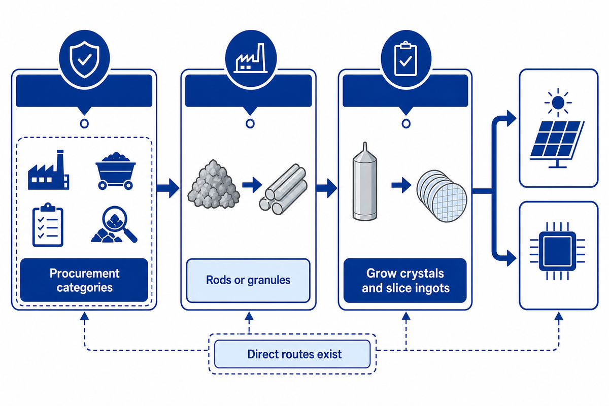
- Conventional solar and semiconductor wafer routes grow crystals and slice ingots, but direct photovoltaic wafer routes and deposited polycrystalline-silicon films are real exceptions.
- In the United States, new polysilicon import measures were signed on August 6, 2026 and are scheduled to take effect on December 4, 2026.
What Is Polysilicon Material?

Polysilicon is a high-purity form of elemental silicon made of many small silicon crystals. Silicon and polysilicon are therefore related terms, but they are not equally specific. In the bulk supply chain, polysilicon is a raw material that comes after metallurgical-grade silicon has been chemically purified and before a manufacturer grows a controlled crystal for wafers.
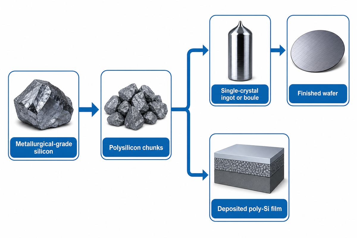
That position in the process is the simplest way to avoid a common category error: polysilicon feedstock, a single-crystal ingot, a finished silicon wafer, and a deposited polycrystalline-silicon film are related materials, but they are not interchangeable products, and assuming otherwise creates qualification risk.
U.S. Department of Energy guidance describes commercial polysilicon production in rod and bead forms. Rods from the Siemens process are typically broken into polysilicon chunks for charging a crystal-growth furnace. Granular product from a fluidized bed reactor can offer a different feeding form. Neither form, by itself, proves that the material meets a buyer’s impurity, doping, traceability, or crystal-growth requirements.
| Material state | それが何であるか | Typical next operation | Procurement boundary |
|---|---|---|---|
| Metallurgical-grade silicon | An upstream industrial silicon source with impurity levels too high for direct use in most wafer production | Chemical conversion and purification | Do not infer solar- or electronic-grade suitability from total silicon content |
| Purified volatile silicon precursor | A distilled silicon-bearing gas such as trichlorosilane or silane used before deposition | Chemical vapor deposition | It is a process intermediate, not solid polysilicon feedstock |
| Deposited polysilicon rod | Elemental silicon deposited on heated seed rods in a qualified reactor process | Controlled cooling, removal, and breakage | Reactor-route identity does not replace lot-specific impurity evidence |
| Polysilicon chunks | Qualified pieces produced by breaking deposited rods under controlled handling | Furnace charging for crystal growth | Specify size distribution, fines, surfaces, packaging, and traceability |
| Granular polysilicon | Purified silicon deposited as granules rather than as a rod | Qualified storage and furnace charging | Granular form does not prove electrical or chemical equivalence to chunks |
| Single-crystal ingot or boule | A crystal grown under controlled thermal and doping conditions | Shaping, orientation, and wafer slicing | Properties now reflect both feedstock and crystal-growth history |
| Finished wafer | A sliced and processed substrate for solar-cell or semiconductor fabrication | Cell or device manufacturing | Wafer geometry and electrical values cannot be copied back onto raw feedstock |
| Deposited poly-Si film | A polycrystalline-silicon layer deposited on an existing chip or wafer | Device-layer patterning or further fabrication | This film route is outside the bulk crystal-growth feedstock scope |
キーテイクアウト: “Polysilicon” identifies a material family and process position; the purchase specification must identify the exact state and intended conversion step.
Polysilicon Material Uses: What Is Polysilicon Used For?
Most bulk polysilicon supports crystalline solar photovoltaic manufacturing, where it becomes ingots, wafers, solar cells, and modules. A smaller, technically demanding share supports electronic-grade crystal growth for integrated circuits, power devices, sensors, and other semiconductor products. Polycrystalline silicon can also be deposited as a thin film for transistor gates, conducting layers, and related device structures. That deposited use should be described separately because it does not follow the bulk-feedstock-to-ingot route.
How Is Polysilicon Made?

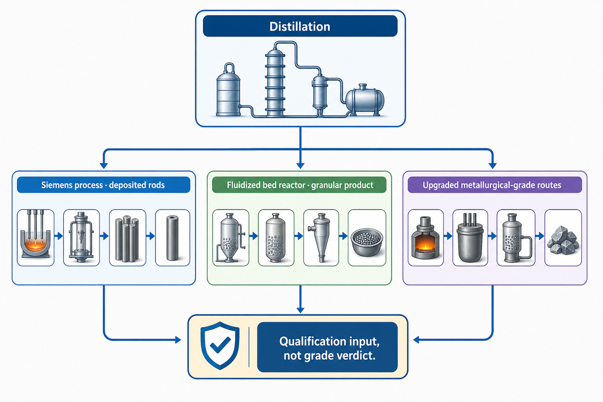
の The polysilicon manufacturing process first converts a silicon source into a volatile silicon compound that can be purified by distillation, then deposits purified silicon under controlled conditions. A common chain reacts metallurgical-grade silicon with hydrogen chloride to form trichlorosilane; silane is used in other qualified deposition routes. Distillation separates unwanted compounds, and chemical vapor deposition turns the purified gas back into elemental silicon. Process design also has to manage hydrogen, silicon tetrachloride, energy use, contamination, and recycled streams.
Siemens process: deposited rods
In the Siemens process, trichlorosilane and hydrogen enter a heated reactor. Silicon deposits on slender seed rods, which grow into larger high-purity rods. After cooling and controlled handling, the rods can be broken into feedstock sizes. This route is widely used because it can support tight impurity control, but the label “Siemens” does not replace a lot certificate or a qualified receiving test.
Fluidized bed reactor: granular product
A fluidized bed reactor, often shortened to FBR in supplier documents, suspends small silicon seed particles in a gas stream while silicon deposits on them. Its output is granular rather than a rod that must be broken. Continuous operation and feeding behavior can be attractive, but granule size distribution, surface condition, contamination control, gas chemistry, and compatibility with the buyer’s charging system still require approval.
Upgraded metallurgical-grade routes
Upgraded metallurgical-grade silicon, or UMG, uses metallurgical purification steps to reduce impurities without copying the complete chlorosilane deposition route. It can be relevant to selected solar applications, blends, or cost and energy studies. It is not automatically equivalent to virgin feedstock governed by a solar specification, and it should never be represented as electronic grade without direct evidence from the intended crystal and device process.
| Route | Typical product form | Useful buyer question | Claim to avoid |
|---|---|---|---|
| Siemens process | Rods, then chunks | Which trace impurities, surfaces, handling controls, and size classes are certified? | Every Siemens lot has the same purity or crystal-growth result |
| Fluidized bed reactor | Granules | How are particle size, fines, surface contamination, and charging behavior controlled? | Granules are always cheaper, cleaner, or electrically equivalent |
| Upgraded metallurgical-grade route | Route-specific pieces or feedstock | Is this material permitted by the receiving process, blend rule, and current specification? | Total silicon percentage proves wafer usability |
| Recycled or recovered source | Route-dependent | What was the source, purification path, segregation rule, and contamination history? | Recovered automatically means lower impact or qualified quality |
キーテイクアウト: A production route explains how the material was made; only evidence tied to the lot and receiving process shows whether it can be used.
Solar Grade vs Electronic Grade: What Purity Controls Change?

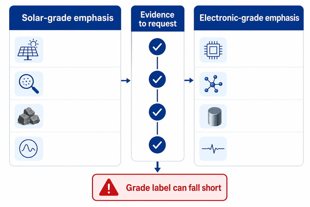
Solar grade and electronic grade differ mainly in the impurity control and process assurance required by their downstream crystals and devices. There is no single global table in which one “nines” value makes every solar lot acceptable and a higher value makes every semiconductor lot acceptable. Procurement works better when the buyer names the impurity species, measurement method, unit, specimen preparation, sampling plan, and acceptance limit.
SEMI PV17’s public scope covers virgin silicon feedstock for photovoltaic crystal growth and distinguishes production routes and excluded materials. SEMI M16’s public scope focuses on form and dimensions for polycrystalline silicon and notes that additional physical properties may be added to a purchase specification with suitable test methods. Together, these boundaries explain why a grade label alone can fall short.
| Decision area | Solar-grade emphasis | Electronic-grade emphasis | 要求する証拠 |
|---|---|---|---|
| End use | Qualified photovoltaic crystal and cell architecture | Qualified semiconductor crystal, wafer, and device flow | Receiving-process specification and approved material list |
| Impurities | Dopants, transition metals, carbon, oxygen, and other yield- or lifetime-relevant species | Tighter device-specific control of electrically active and metallic contaminants | Named elements, limits, units, methods, and detection capability |
| Product form | Chunks, rods, granules, or another accepted feed form | Form, dimensions, surfaces, and handling matched to crystal growth | Size distribution, surface specification, packaging, and lot traceability |
| Electrical target | Matched to the planned p-type or n-type crystal and solar cell | Matched to device resistivity, doping, lifetime, and defect requirements | Agreed property method and the stage at which it applies |
| Change control | Source, route, equipment, packaging, and blend changes reviewed before use | Formal notification and requalification for sensitive changes | Supplier change-notice terms and retained-sample plan |
SEMI PV49’s public scope is a useful example of what a test method adds. It names bulk-digestion inductively coupled plasma mass spectrometry for specified elemental impurities in photovoltaic silicon feedstock and states an approximate range of 0.1 to 10,000 micrograms per kilogram. This does not create a universal acceptance limit. It shows that a meaningful requirement identifies what is measured and how.
Who makes the purest polysilicon?
A defensible answer cannot be obtained from supplier marketing alone, because “purest” changes meaning with the receiving process and analytical method. No public evidence supports a universal supplier ranking across every impurity matrix, test method, product form, and receiving process.
Phrases such as “hyper-pure polysilicon” or “pure silicon” may refer to total measured impurities, selected electrically active elements, surface metals, carbon, oxygen, lot consistency, or suitability after a particular crystal-growth route; a result without a specimen state, detection limit, and sampling location cannot support a fair comparison. Buyers should compare current certificates produced with comparable methods, audit the sampling and detection rules, and confirm downstream crystal results across more than one qualified lot when continuity matters. A manufacturer can lead on one impurity matrix without being the best-qualified source for every application, so the better question is which supplier has demonstrated the buyer’s complete acceptance matrix and change-control requirements.
Properties That Matter Before Crystal Growth

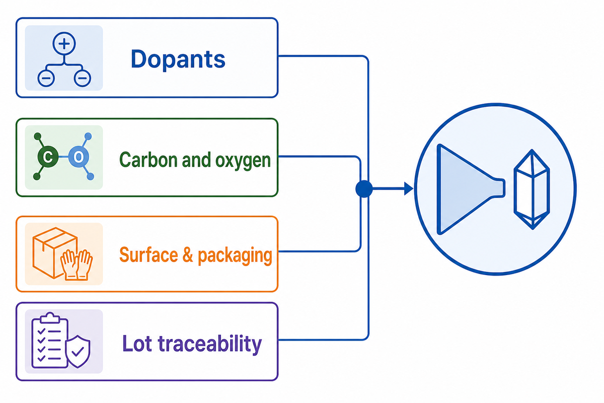
Polysilicon material properties that matter are the ones that can change crystal behavior, wafer yield, or device performance. Resistivity is a good warning against copying a single number: a National Institute of Standards and Technology publication documents that electron mobility and resistivity in n-type silicon depend on dopant density and temperature. Material state and test condition therefore belong beside the value.
- Dopants such as boron and phosphorus can shift conductivity type and resistivity; the acceptable balance depends on the intended crystal.
- Selected transition and alkali metals can affect carrier lifetime, junction behavior, or defect formation even when total purity looks impressive.
- Carbon and oxygen must be evaluated by source, chemical form, process evolution, and detection method. An industry-affiliated 2026 HSC simulation study examines how carbon-containing species evolve during the modified Siemens process, so its findings should be interpreted within that process scope.
- Particle or chunk form includes size distribution, fines, sharp edges, packing behavior, surface area, and charging behavior that can affect handling and contamination risk.
- Surface and packaging controls matter because a clean bulk analysis does not excuse contaminated breakage, packaging, transport, or furnace charging.
- Traceability includes lot identity, reactor or campaign history, sampling location, method revision, and change control.
Prepared wafers and feedstock should normally be treated as different specimens. One controlled exception makes the boundary clearer: the public SEMI PV25 scope describes a secondary ion mass spectrometry method for oxygen, carbon, boron, and phosphorus in both prepared wafer and feedstock samples. Comparable data may be possible when preparation, method, range, and specimen state are aligned. It is still unsafe to copy an arbitrary wafer value onto raw chunks.
Terminology and Quantitative Evidence Map
Polysilicon terminology often mixes a production process, a form of silicon, an end market, and a legal threshold. This map keeps those categories apart. It also supplies traceable numerical reference points without turning them into universal purchase limits.
| カテゴリー | Term or published value | What it can establish | What it cannot establish |
|---|---|---|---|
| 1. Upstream source | Silicon metal and metallurgical silicon | The industrial source that can enter purification | Suitability for a wafer process |
| 2. Purification action | Produce polysilicon; production of polysilicon | Conversion and purification create a high-purity form of silicon | One route or certificate fits every buyer |
| 3. Siemens output language | Silicon rods, silicon filaments, and silicon fragments | Seed geometry, deposited rod, and broken feed descriptions | That every fragment has the same surface history |
| 4. Granular language | Silicon particles and multiple small silicon crystals | Why granular feed behaves differently in storage and charging | Automatic equivalence to rod-derived chunks |
| 5. Solar sector | Polysilicon for solar, solar silicon, solar PV, solar energy, renewable energy, solar modules, and PV manufacturers | The commercial chain from feedstock to production of solar cells and cell manufacturing | A technical grade or impurity limit |
| 6. Crystal route | Crystalline silicon, molten silicon, and material cast into multicrystalline ingots | The transformation from bulk feedstock to an ingot | That all photovoltaic routes require sawing |
| 7. Device route | Electrical properties and semiconductor chips | The downstream reason for tight doping and contamination control | That bulk feedstock alone fixes final device behavior |
| 8. Supplier and cost context | Polysilicon producers, the polysilicon market, polysilicon manufacturing, and manufacturing costs; Wacker is one named producer | Commercial research categories and supplier identity | A purity ranking or source approval |
| 9. NIST electrical-property boundary | Electron mobility and resistivity depend on dopant density and temperature | Why an electrical value needs a stated material condition and test context | A raw polysilicon lot specification |
| 10. NIST deposited-film context | Doped and undoped amorphous or polycrystalline silicon can be deposited on chips and existing wafers | A separate semiconductor use of poly-Si | Bulk crystal-growth feedstock equivalence |
| 11. U.S. tax definition | 99.999999% silicon by mass and a $3/kg credit amount | The specific Section 45X solar-grade definition and credit | A global engineering threshold or market price |
| 12. U.S. photovoltaic wafer definition | At least 240 cm² and a $12/m² credit amount | The statutory component boundary and credit | A recommended wafer size or sales price |
| 13. Other Section 45X values | $0.04/W for a photovoltaic cell, $0.07/W for a solar module, and $0.40/m² for a polymeric backsheet | Why legal values must stay attached to their component | A feedstock property or manufacturing-cost model |
| 14. SEMI PV49 control | 75% to 125% certified-reference-material recovery in the public method scope | A method performance check within that scope | The buyer’s impurity acceptance limits |
| 15. DONGHE first-party example | 0.04 mm to 0.25 mm stated wire-diameter range for MW2318 | A declared machine-family capability range | The correct wire for a particular wafer |
| 16. U.S. 2026 import schedule | $21/kg polysilicon, $100/kg ingots and wafers, $0.22/W cells, and $0.38/W modules | The values in the signed U.S. action scheduled for December 4, 2026 | Global spot prices or technical grades |
| 17. Attributed policy findings | More than 270% production growth since 2020, about 400,000 tons of inventory at the end of 2024, and semiconductor-grade material at 2.4% of global polysilicon production | Findings stated in the 2026 policy record | Independent consensus or a forecast |
These comparisons are intentionally non-equivalent. A $21/kg import floor is not the $3/kg tax credit, and a $12/m² wafer credit is not a wafer price. Likewise, the 99.999999% statutory definition does not replace the 75% to 125% method-recovery check or the buyer’s element-by-element limits. Numerical evidence becomes useful only when its owner, unit, date, material state, and purpose stay attached.
What are the disadvantages of polysilicon?
Bulk polysilicon is energy- and equipment-intensive to purify, and its quality can be degraded by contamination during deposition, breakage, packaging, transport, or charging. It is also an intermediate rather than a finished substrate, so downstream crystal growth, shaping, slicing, and finishing add cost and yield risk. Market concentration and trade rules can create sourcing exposure. These disadvantages vary by production route, energy source, product form, location, and qualification burden; they should not be collapsed into an environmental or cost claim.
How Polysilicon Becomes Solar Wafers and Cells

で conventional crystalline solar route, qualified polysilicon is charged into a furnace, melted, and grown into a monocrystalline ingot or solidified into multicrystalline material. The ingot is shaped and sliced into silicon wafers. Wafer cleaning, texturing, junction formation, passivation, metallization, and testing then create a solar cell, and interconnected cells become a solar panel or module.
- Incoming qualification: verify lot identity, feed form, impurity certificate, packaging, and approved source status.
- Crystal growth: set charge composition, dopants, atmosphere, thermal history, and growth method for the intended crystal.
- Ingot preparation: crop, orient, shape, and inspect the crystal before slicing.
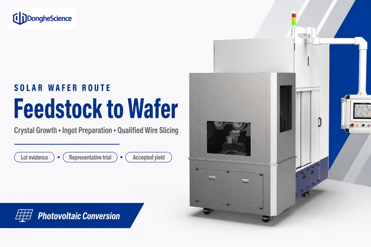
- Wafering: use qualified diamond wire saw machines and wire conditions to control thickness, kerf, bow, surface damage, breakage, and accepted yield.
- Cell and module manufacturing: convert accepted wafers into cells, interconnect them, laminate the stack, and test the finished module.
DONGHE’s first-party MW2318 catalog lists monocrystalline and polycrystalline silicon among the supported materials and states a 0.04–0.25 mm wire-diameter range. That is a machine-family example, not an industry-wide recommendation. Actual wire diameter, pitch, feed, tension, fluid, and acceptance limits must be matched to the wafer target and validated on representative material.
Not every photovoltaic wafer requires an ingot to be sliced. The U.S. Internal Revenue Service’s final-regulation discussion recognizes photovoltaic wafers made by forming an ingot and slicing it, by forming molten or evaporated solar-grade polysilicon directly into a sheet or layer, or by thin-film deposition. Direct and kerfless routes are therefore genuine exceptions, even though ingot-and-wire-slicing remains the mainstream chain addressed by most bulk feedstock purchases.
キーテイクアウト: The value of polysilicon is realized only after the crystal and wafer process converts it into accepted wafers; feedstock quality and slicing quality belong to one traceable yield chain.
How Polysilicon Enters Semiconductor Manufacturing

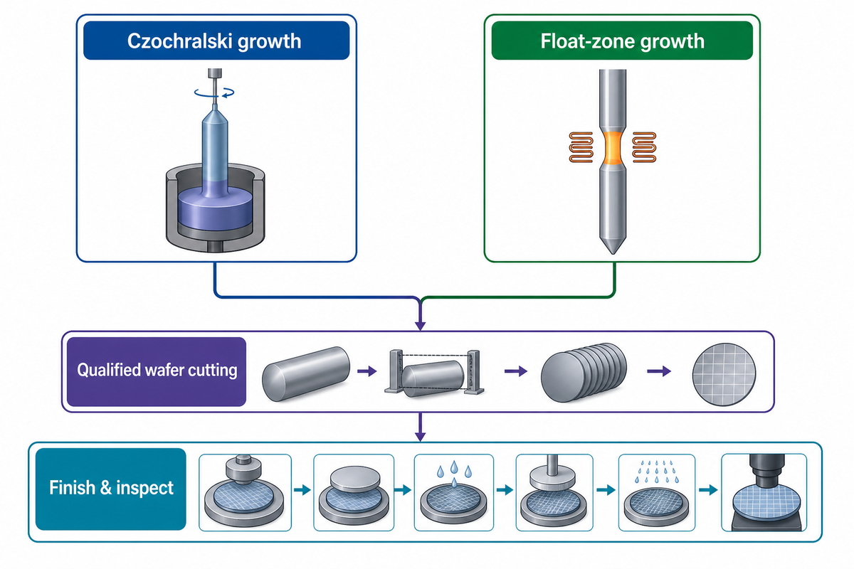
Electronic-grade bulk polysilicon usually enters a more tightly controlled single-crystal route. Czochralski growth melts feedstock in a crucible and pulls a crystal from the melt. Float-zone growth moves a molten zone through a polysilicon rod without a crucible, creating a different contamination and oxygen boundary. The choice affects far more than the feedstock label.
After growth, the boule is oriented, shaped, sliced through a qualified silicon wafer cutting process, lapped, etched, polished, cleaned, and inspected before device fabrication. Dopant distribution, oxygen, carbon, defects, resistivity, orientation, flatness, thickness variation, surface particles, and crystal-growth history can all matter. A feedstock certificate is necessary evidence, but it cannot guarantee the finished wafer because the growth and finishing steps introduce independent variables.
There is also a second semiconductor meaning of polycrystalline silicon. The NIST NanoFab documents amorphous and polycrystalline silicon deposited directly on chips and existing wafers, with doped and undoped options for conducting layers, transistor gates, and related structures. This deposited poly-Si is a device-fabrication film, not a bag of crystal-growth feedstock. An article or request for quotation should state which meaning is intended.
Polysilicon vs Monocrystalline and Amorphous Silicon

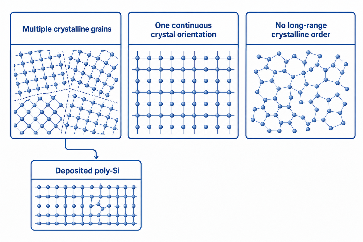
The difference is crystal structure and production state. Polysilicon contains multiple crystalline grains. Monocrystalline silicon has one continuous crystal orientation across the relevant solid. Amorphous silicon lacks long-range crystalline order. The same element can therefore serve different roles depending on how it was purified, formed, grown, or deposited.
| 材料 | Structure or form | Representative use | Important boundary |
|---|---|---|---|
| Bulk polysilicon | Many grains; rods, chunks, or granules | Starting material for photovoltaic or electronic crystal growth | Grade is proven by a scoped specification, not the word “poly” |
| 単結晶シリコン | Controlled single crystal | Solar wafers and semiconductor substrates | Finished properties reflect growth, doping, and wafer processing |
| Multicrystalline silicon | Solid containing multiple larger crystal regions | Selected crystalline solar wafers | Do not confuse a cast ingot or wafer with purified feedstock chunks |
| Amorphous silicon | No long-range crystal order; often a deposited film | Thin-film photovoltaic and electronic layers | Its deposition route is outside conventional bulk wafer growth |
| Deposited poly-Si | Polycrystalline film on a substrate | Gates, conductors, and device structures | It may be doped during deposition and never become a sliced ingot |
Polysilicon-to-Wafer Qualification Chain

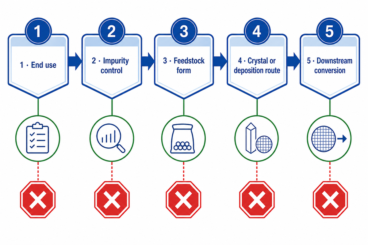
A buyer should clear five gates before accepting a polysilicon source: end use, impurity control, feedstock form, crystal or deposition route, and downstream conversion.
A purity percentage describes chemistry; a usable grade also describes evidence, handling and downstream qualification.
The framework prevents a low-information statement such as “11N material required” from replacing the evidence the factory actually needs.
| ゲート | Question | Evidence to collect | Stop condition |
|---|---|---|---|
| 1. End use | Which solar cell, semiconductor device, or deposited-film flow will receive the material? | Drawing, process owner, approved material class, electrical target, and governing purchase document | The supplier cannot identify the intended material state or receiving flow |
| 2. Impurity control | Which elements and forms can damage the crystal, wafer, cell, or device? | Element-by-element limits, units, methods, detection limits, specimen preparation, sampling, and lot certificate | Only total purity or an unsupported “nines” label is provided |
| 3. Feedstock form | Can rods, chunks, granules, or another form enter the charge and handling system safely? | Dimensions, particle distribution, fines, surface condition, packaging, traceability, and contamination controls | The form or packaging conflicts with the validated charging process |
| 4. Crystal or deposition route | Will the material be used in Czochralski, float-zone, multicrystalline, direct-wafer, or thin-film deposition? | Route-specific source approval, dopant plan, thermal history, crucible boundary, blend rule, and change notice | Suitability is inferred from another route without qualification |
| 5. Downstream conversion | Can the resulting ingot, wafer, film, cell, or device meet accepted yield and quality? | Representative trial data across growth, slicing, cleaning, and downstream tests; rejection and requalification rules | No traceable link exists between feedstock lot and accepted downstream output |
Turn the matrix into a request for quotation by attaching the receiving specification, planned route, lot size, certificate template, sampling plan, packaging rule, change-notice period, and trial acceptance criteria. The supplier should fill gaps with evidence or state that a requirement is not currently demonstrated. An honest gap is safer than an invented grade equivalence.
What Is Changing in Polysilicon Supply and Sourcing?

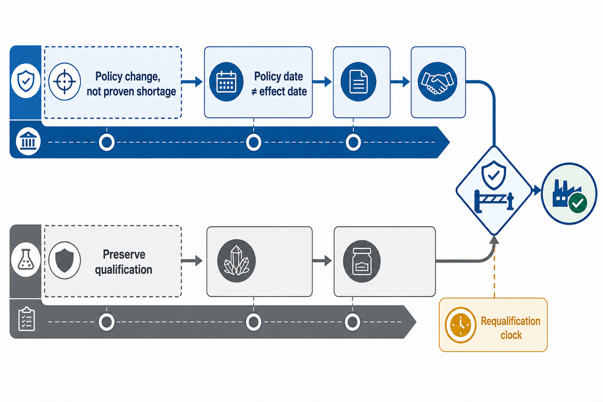
The immediate 2026 change is policy, not a proven global shortage. A U.S. proclamation signed August 6, 2026 establishes a minimum import price of $21 per kilogram for polysilicon and related measures scheduled to take effect December 4, 2026. The document also reports large production and inventory changes. Those market figures are findings of the policy document and should remain attributed rather than presented as neutral consensus.
For a buyer, the practical response is to map country of origin, first arm’s-length sale documentation, derivative classification, existing contracts, inventory timing, and alternative qualified sources. A rapid source change can create a technical problem even when it solves a customs or price problem. Receiving specifications, change control, crystal trials, and retained samples should move with the commercial review.
- Separate the policy date from the effect date: August 6 is the signing date; December 4, 2026 is the scheduled start date.
- Preserve technical qualification and do not substitute an unapproved lot solely because its delivered price is lower.
- Review origin and documentation with qualified trade and legal advisers for the actual transaction.
- Model both directions: producer support may improve domestic capacity while higher input cost may affect solar and semiconductor buyers.
- Keep a requalification clock because source, route, form, packaging, or process changes may require testing before production use.
よくある質問frequently Asked Questions
Is polysilicon the same as silicon?
Polysilicon is elemental silicon in a polycrystalline form, so it is silicon, but the terms are not equally specific. “Silicon” can also refer to metallurgical material, a single-crystal wafer, a multicrystalline ingot, an amorphous film, or a compound-bearing product. A technical document should identify purity, structure, material state, and intended process.
Is polysilicon expensive?
Its cost changes with grade, region, contract terms, energy, route, product form, qualification, and market cycle. Spot prices are not a safe budget for electronic-grade qualified supply, and a low feedstock price can be erased by poor crystal or wafer yield. Compare delivered and qualified cost per accepted downstream unit.
Can solar-grade polysilicon be used for semiconductor wafers?
Not by assumption. Some source streams, equipment, or upstream operations may be related, but a semiconductor crystal and device flow can require different impurity, consistency, traceability, and change-control limits. A supplier’s solar-grade certificate may omit an electrically active contaminant, surface-metal limit, sampling rule, or process-change notice needed by the semiconductor buyer. Crystal growth also matters: Czochralski and float-zone routes create different oxygen and contamination boundaries. Use is allowed only when the receiving specification accepts the exact source and form, comparable methods verify the required impurities, and representative crystal, wafer, and device evidence passes the agreed qualification plan.
Which country produces the most polysilicon?
China holds the dominant share of current global solar manufacturing capacity, while qualified production also exists in other regions. The exact share changes with capacity, utilization, closures, and the definition used. For sourcing, country-level capacity is less useful than the approved plant, route, lot evidence, origin record, and continuity plan.
Is there a polysilicon shortage?
There is no single global yes-or-no answer. Total solar-grade capacity can be ample while a region, electronic-grade specification, approved source list, origin rule, or product form remains constrained. Check current inventory, qualified capacity, logistics, policy exposure, and your own requalification lead time.
Does polysilicon become a wafer directly?
Usually, bulk feedstock first becomes a controlled crystal or ingot and is then sliced. Direct and kerfless photovoltaic technologies can form a sheet or layer without the conventional ingot-slicing sequence, and deposited polycrystalline-silicon films are made on an existing substrate. State the route before answering.
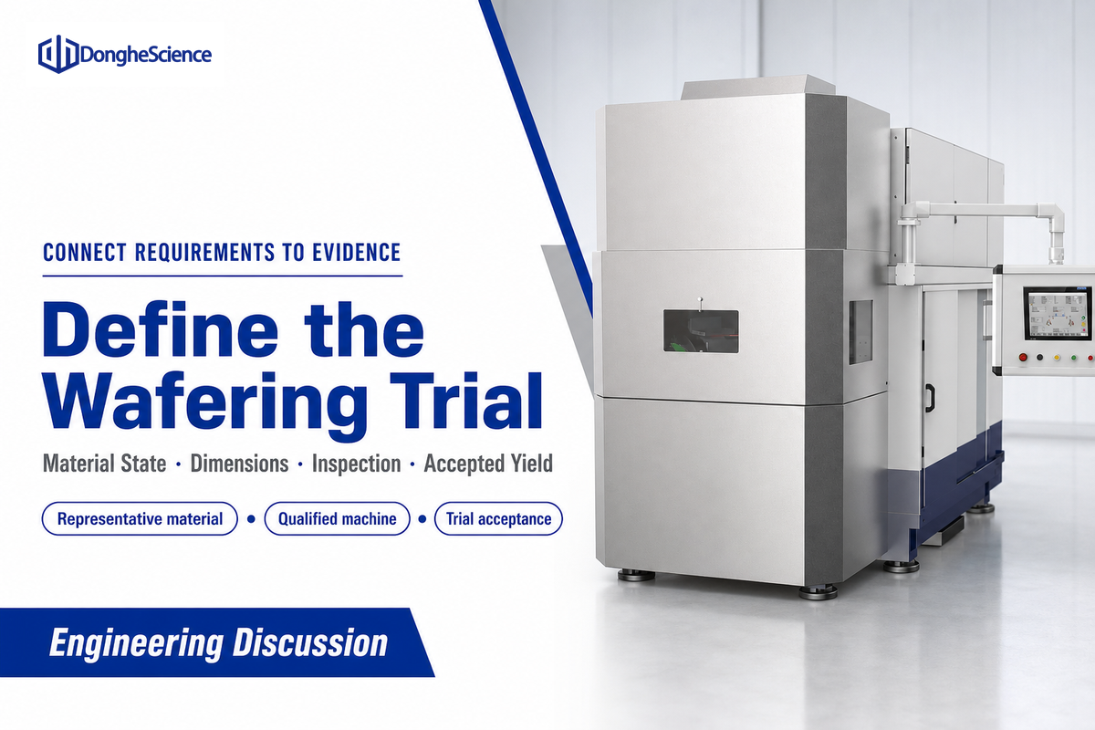
Connect Feedstock Requirements to Wafering Evidence

Send DONGHE the material state, ingot or wafer dimensions, target thickness, surface and edge criteria, throughput pattern, inspection method, and accepted-yield definition. The engineering discussion can then connect the downstream cutting requirement to a qualified machine and trial plan.
参考文献と情報源
- U.S. Department of Energy. Solar Photovoltaic Manufacturing Basics. Manufacturing route and material-state background.
- Brigham Young University Integrated Microfabrication Laboratory. Electronic Wafer Formation. Conventional semiconductor crystal and wafer process.
- SEMI. SEMI M16 public specification page. Public scope only.
- SEMI. SEMI PV17 public specification page. Public scope only.
- SEMI. SEMI PV49 public test-method page. Public scope only.
- SEMI. SEMI PV25 public test-method page. Public scope only.
- Hou, Y.; Lv, X.; Huang, G. Study on the Evolution Mechanism of Carbon Impurities in Polysilicon Production Based on HSC Simulation, 材料 19(4):798, 2026. Two authors reported employment by Xinjiang Xinte Crystalline Silicon High-Tech Co., Ltd.; interpret the process findings with that disclosed industry connection.
- National Institute of Standards and Technology. Dopant Density and Temperature Dependence of Electron Mobility and Resistivity in N-Type Silicon.
- National Institute of Standards and Technology NanoFab. LPCVD Amorphous and Polycrystalline Silicon. Deposited-film scope.
- Internal Revenue Service. Internal Revenue Bulletin 2024-51. Final-regulation discussion of photovoltaic wafer routes.
- The White House. Adjusting Imports of Polysilicon and Its Derivatives Into the United States, August 6, 2026.
- Reuters. U.S. weighs polysilicon price floor and tariffs, August 4, 2026. Dated trade-off context predating the signed action.