DONGHE Company に連絡してください


ウェーハ製造装置は、成長したシリコン結晶インゴットを完成した研磨された裸のウェーハに変えるフロントエンドマシンのセットです ⁄チップファブが後で回路を構築する基板 ウェーハライン用のツールを調達している私たちのほとんどにとって、最初に知っておく価値があるのは、これはチップをパターン化するウェーハファブ装置 (WFE) と同じサプライチェーンの半分であり、おそらくその一部だけツールを購入する必要があるということです。.
このガイドでは、インゴットからウェーハへのツールチェーン全体をプロファイルします。このプロファイルは、マーケティング誇大宣伝ではない実際の仕様 (kerf、TTV、表面粗さ、表面下の損傷など) を提供し、1 つの意味のある数値、つまり Cost Per Good Wafer (CPGW) 値のみを含む購入決定プロセスを提供します。これは、ウェーハ フォーム ファクターに続くすべてのプロセスで歩留まりに最終的な制限を課す隠されたステップを特定し、その正当性を示します。このステップの多くは、当社のベンダーのどれも開示していません。.
クイックスペック: 一目でわかるウェーハ製造装置
| プロセススコープ | 結晶成長→トリミング/ODグラインド→ワイヤーソースライシング→エッジグラインド→ラッピング→エッチング→研磨/CMP→洗浄+計測 |
| 標準ウェーハサイズ | 100 / 150 / 200 / 300 mm メインストリーム; 450 mm 標準化されましたが、停止しました |
| 典型的な300 のmmの厚さ | 公称約 775 μm (200 mm: 725-775 μm) |
| ダイヤモンドワイヤーカーフ損失 | ~70-150 µm (対~180-220 µm スラリーマルチワイヤー) |
| グッドウェーハTTVターゲット | 1 桁の µm (スライスされたまま); SEMI M1 に保持された平坦度 |
| 準拠規格 | SEMI M1 (研磨された単結晶シリコン ウェーハ)、現在のファミリーには M1-0114 が含まれます |
Wafer Manufacturing Equipmentとは?
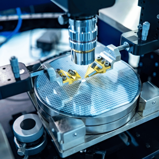
ウェーハ製造装置は、単結晶シリコンインゴットを完成したベアウェーハ ⁄ 結晶成長、スライス、研削、ラッピング、エッチング、研磨、クリーンに変換するツールのフロントエンドセットです。ウェーハ製造装置 (WFE) は、フォトリソグラフィー、エッチング、堆積、平面化など、そのベアウェーハ上に集積回路を構築する個別の後のセットです。.
大学 クリーンルーム プログラム 同じ分離を行います。ウェーハの形成は、デバイスを追加する前に、単結晶インゴットを基板に加工することから始まります (切断、研削、研磨、洗浄)。.
そして、商業的には、それは重要です。基板ハウスの購入者は、クリスタルプラー、ワイヤーソー、エッジグラインダー、ラッピングおよび研磨ツール、計測学を必要とします。 ーこれは「ウェーハ製造」の半分です。回路ファブの購入者は、リソグラフィースキャナー、プラズマエッチャー、CVD/ALD堆積装置、CMP ーーこれは、ASML、アプライドマテリアルズ、ラムリサーチなどの大企業によって製造された「チップ製造」の半分を必要とします。この記事では、前者 ーブランクウェーハを製造するためのツールについて説明します。文字通り、ウェーハの製造は基板の準備であり、チップファブはこれらの基板を使用して、現代のエレクトロニクスで数十億個のトランジスタを製造します。.
実際には、ここで最もコストのかかる間違いは調達です。ウェーハ製造の予算を立てているものの、回路製造のように読み取り可能な RFQ を循環させているチームは、2 つのラインがほとんど機器を共有していないため、間違った半分に見積もられています。簡単な修正: プロセス ステップに名前を付ける - RFQ のすべてのラインでスライス、ラッピング、研磨、またはエッチング - するため、775 µm の基板仕様はリソグラフィー スキャナーではなくワイヤーソーにマッピングされます。.
言い換えれば、ウェーハ製造では基板が製造され、半導体製造では完成したチップがパターン化され、収縮するデバイスの形状が周囲の電子デバイスを定義します ――同じ処理シリコンが両方の半分を支えます。.
💡 プロのヒント
見積もりに「ウェーハ製造装置」と記載されている場合、その「半分」とは何かを尋ねます。ウェーハ洗浄ウェットベンチとチョクラルスキー水晶牽引機はどちらも製造機と呼ばれるかもしれません。ただし、この装置はプロセスの非常に異なる部分に設置されており、さまざまな顧客に販売されています。.
インゴットからウェーハまでの機器チェーン: 8 つのプロセス ステップ
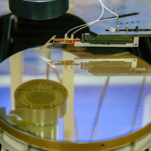
要するに, 約 8 ツール ステーション任意の裸のシリコン ウェーハが見る. 以下のマップ我々はインゴットからウェーハへのスペック ラダーとして参照 -その機能は、よりきつく締められている理由, 真実と一緒に、非常に最初の不完全性は、後に引き戻されることがある場合、かろうじてすることができます -あなたはそれらの基本的な段階が何度もミラーリングされている見つける間 学術的なウェーハ製造のレビュー シリコンウェーハの製造について。.
| ステップ | 設備 | 削除アクション | 出力/許容値が制御されます |
|---|---|---|---|
| 1.結晶成長 | チョクラルスキー (CZ) プラー/フロートゾーン炉 | 溶融物から単結晶インゴットを成長させます | 結晶配向性、抵抗率、直径 |
| 2.トリミング&ODグラインド | インゴットトリミングソー、ODグラインダー | 種子/尾を取り除き、正確な直径に粉砕し、平ら/ノッチを切ります | 最終直径、向きは平らです |
| 3. 針金の鋸スライス | ダイヤモンド マルチワイヤー ソー (またはレガシースラリー/IDソー) | インゴットを1 回のパスで多数のウェーハに切断します | カーフ、TTV、地下損傷 ¤ 収量上限 |
| 4.エッジ研削/ベベリング | エッジグラインダー/ベベルマシン | ウェーハのリムを定義されたプロファイルに丸めます | エッジプロファイル、チップ/クラック抵抗 |
| 5.ラッピング/研削 | 両面ラッパー、ファイングラインダー | 両面を平らにし、鋸の跡を取り除きます | グローバル平坦性、並列性 |
| 6.エッチング | ウェットエッチステーション/ウェットベンチ | 残留ダメージ層を化学的に除去します | 表面の損傷、汚染 |
| 7.研磨/CMP | CMPポリッシャー、化学機械平面化 | ミラー仕上げ、最終平面化を実現します | 表面粗さ (Ra)、ナノトポグラフィー |
| 八 掃除 | シングルウェーハ/バッチクリーナー (RCA タイプの化学) | 粒子、金属、有機物を剥ぎ取ります | 汚染のない表面 |
| 9.計測&検査 | 平坦度、厚さ、欠陥の計測ツール | 対策、材料を除去しません | SEMI M1 への適合性を検証します |
ウェーハ製造とSEMIプロセス分類に関する学術界のレビュー論文に基づいて構築されたプロセススパイン
8 つのステーションすべてがクリーンルームに供給し、フロントエンドのウェーハハンドリングはウェーハから粒子を離さないようにするために大幅に自動化されており、ライン全体にまたがる計測とエッジグラインダーはゲートキーパーとして機能します。ラダーはベンダーがパンフレットで何を覆っているかを明らかにします; ステーション 5 ~ 8 は修正的です。彼らは鋸で作られた混乱を研削、エッチング、研磨し、より滑らかな平らなウェーハを提供しますが、いずれにせよ決してなかった失われた厚さの均一性を取り戻すものではありません。これは、このクラス全体に関する最も重要な点を紹介します。.
実際の生産ラインでは、オペレーターが 9 つのステーションすべてを順番に実行し、順序は容赦ありません。実際には、エッチングが不十分な 1 つのバッチで、ウェーハが下流の 3 つのステーションに亀裂が入るまで現れない 8 ~ 12 μm の地下損傷が残る可能性があります。根本原因は、非難される研磨機ではなく、スライスに直接遡ります。.
ウェーハスライス装置: ワイヤーソーが収量上限を設定する理由
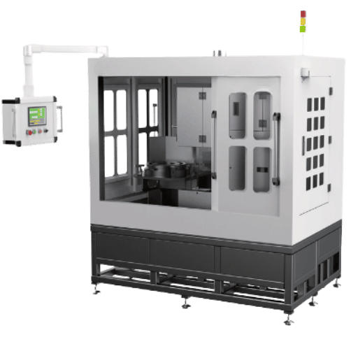
スライスすることは、ウェーハ上で行う最も厳しい、最も高い回収ステップです。私たちの用語は、スライス収率天井です; すべてのスライス後のツール-研磨、測定など-は、可能な限り最高のファーストパス収率に鋸引きTTV、カーフと地下の損傷によって制限されていますあなたはより滑らかに磨く、あなたはバリエーションや鋸切りの下に封印された亀裂を磨くことができませんダイヤモンドスラリーでワイヤーでモノラルSiを切断することに関するピアレビュー記事は、この-脆性モードの材料の除去が必然的に後で切断されなければならない地下の微小亀裂を引き起こすという正確な証拠を提供します。.
シリコンウェーハはインゴットからどのようにスライスされますか?
現代の線はaを切り抜けています ダイヤモンド マルチワイヤー ソー; ダイヤモンドコーティングされた1 本のワイヤーがスロットに沿って何百回も平行して描かれ、インゴット全体を1 つのスライスで通過します。一般的な説明では、ワイヤーソーでスライスしてからウェーハグラインダーで研磨すると言われていますが、最も重要なのは、ソーが後に残すもの ⁄ カーフ、総厚さの変動、損傷の深さ ⁄ 操作全体の歩留まりを決定します。.
これら 3 台の鋸盤はミクロンレベルの違いによって競合します。.
| スライス方法 | カーフ損失 | スループット | ベストフィット |
|---|---|---|---|
| ID(内径)のこぎり [レガシー] を | 高い; カットごとに1 つのウエファー | 最低 | 専門 / 非常に大きい直径のみ |
| 緩い研摩のスラリーの多ワイヤー | ~180-220μm | 高い(多くのウエハース/パス) | 硬質/脆性化合物、ワイヤーコストを低減 |
| 固定研磨ダイヤモンドマルチワイヤー | ~70-150μm | 最高、よりクリーンなカット | シリコン&ほとんどのSiC; TTVが低く、汚染が少ない |
Kf および TTV は、業界全体の太陽光発電および半導体スライシング データを使用した方程式開発から採用されています。ダイヤモンドマルチワイヤー実装からのフィールドデータ。.
しかし、結果は測定可能です: フィールドトライアル中に、現在レガシーIDソーイングを使用しているある基板サプライヤーは、新しい半導体グレードのダイヤモンドマルチワイヤソーを実装し、その後、生産実行全体での改善を定量化しました:
12-15 → 4-6 μm
TTV(-63%)
180→75μm
カーフ (-58%)
82% → 96.5%
ファーストパス利回り
その後、地下の損傷は25-35 µmから8-12 µmに低下し、機械出力は同じラインで1 台あたり180 から520 のウエハーに上昇しました。 sawでのTTVが低いと、その後のラッピングと研磨は修復する表面が少なくなります ーそれはまさに天井の目的です: スライスに投資し、下流のすべてのことが簡単になります。 DONGHEのダイヤモンドマルチワイヤーソーは、この切断ステーションの機械であり、あなたが私たちのさらなる書き込みを読んだ場合 シリコンウェハ 切断 ワイヤソー 50 µm 以下のダイヤモンド ワイヤーが縁石を 60-80 µm まで下げる方法を学びます。.
“「硬くても脆いSiC素材のウェーハ研削、CMP、研磨パッド、スラリーに大幅な変更が加えられています。」”
半導体工学、「超硬シリコン時代の電力セミの到来」“
ウェーハのサイズと装置:200mm対300mm対450mm
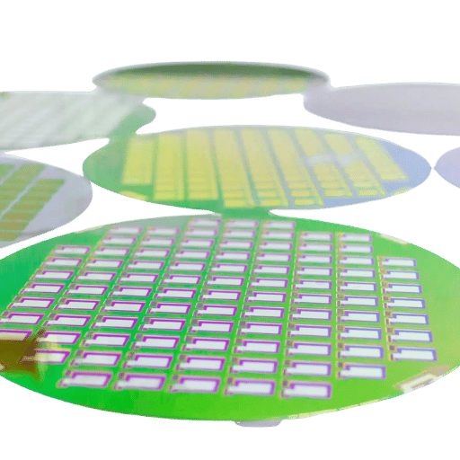
ウェーハターゲット直径は、ライン内の1 つのツールから次のツールへと進化します この方程式では、より大きな方が優れています より広いとは、ウェーハあたりのダイ数が多いことを意味しますが、インゴット直径、ワイヤウェブ直径、カット時間、および取り扱いにおいて最も人気のあるウェーハサイズです SEMI によって定義されます:100、125、150、200、300、450 ミリメートル.
| ウエハサイズ | 公称厚さ | 機器 含意 | ステータス |
|---|---|---|---|
| 200 のmm (8 の″) | 725-775μm | 成熟したツーリング;パワー&アナログ、MEMSに好まれています | 専門に人気 |
| 300 のmm (12 の″) | ~775μm | 高いオートメーション、より広いワイヤー網、より重いインゴット | ボリュームスタンダード |
| 450 のmm (18 の″) | ~925 µm (提案) | 標準化(例:SEMI M1-0114)されているが、ボリュームツーリングなし | 行き詰まった |
これらも自動化を推進します。 300 mm を実行すると、ラインは完全に自動化されたウェーハ処理とロボット カセット処理機能に移行します。 - 半自動モードから完全に自動化されたモードに移行する 200 mm ラインはほとんどありません。自動化を増やすと、一貫性が向上し、生産ライン全体を通じて高い収率が持続します。したがって、大量生産 300 mm 生産ラインでは、一般的に手動ウェーハ処理を回避します。重要な洞察: 移行を正当化するには、プレステージではなくデバイスとボリュームに直径を一致させる必要があります。 450 mm 移行は何年も前に標準化されましたが、経済性はまだ解決されていないため、200 mm がパワー デバイスと研究の基礎を保持している間は、300 mm が依然として大量の主力製品です。最終的に、ウェーハ直径はワイヤソーのウェブ幅のサイズを定義し、使用するロボット工学と計測の処理、およびクリーン ルームの設置面積を定義します。したがって、ウェーハ サイズはおそらく、最初に行われるテクノロジーの決定です。.
より大きな直径はインゴットの質量とワイヤーウェブの幅を一緒にスケーリングするため、新しい 300 mm ラインの解像度は、初日から 775 μm のウェーハに合わせてハンドリング ロボット工学と計測学のサイズを調整することです。実際には、200 mm の機械工場を 300 mm に改造すると、鉛筆が抜けることはほとんどなく、スループットの計算と 725 ~ 775 μm の厚さウィンドウの両方が同時にシフトします。.
良いウェーハをスクラップから分離するスペック: TTV、カーフ、ラー、ダメージ深さ
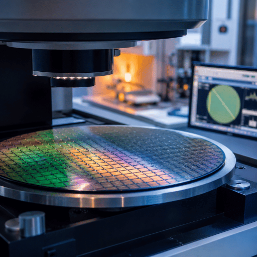
紙上の 4 つのウェーハ テスト データ ポイントは、ウェーハの船舶またはスクラップを予測できます。これら 4 つの数値の読み方 = と、どのツールがそれらを測定するかを知っていれば、その「高精度」機器の見積もりを読むときに、より情報に基づいた決定を下すことができます。.
| Spec | それが何であるか | なぜそれが重要なのか | 制御ステップ |
|---|---|---|---|
| TTV (総厚さの変化) | ウェーハ全体の最大マイナス最小厚さ | リソグラフィーの焦点深度を駆動します。高い TTV = スクラップ | スライスしてからラップします |
| カーフ | スライスごとの切断幅として失われた材料 | カーフが低くなる = インゴットあたりのウェーハが多くなる = コストが低くなります | スライス(ワイヤー直径) |
| Ra(表面粗さ) | 研磨面の平均粗さ | ボンディング/リソグラフィーの品質を設定します | 研磨/CMP |
| 地下損傷の深さ | 切られた面の下の埋もれた微小亀裂の深さ | 完全に取り外すか、破損するまで伝播する必要があります | スライス;エッチング/ポリッシュで削除 |
嬴工注
平坦性とナノトポグラフィーは両方とも、研磨された単結晶シリコンウェーハ仕様の定義である SEMI M1 に制御されます。 (今日では、おそらく SEMI M1-0114 のように現在のファミリーが欲しいでしょう。)弓と経糸は、おそらく総厚さの変動とは別に、個別に制御します 国家計量学の推奨事項 とシリコンを制御する手順. acceptability limit を確立するとき, 全体の平坦性だけでなく、サイトの平坦性が必要です. what your stepper controls is site flatness; it sees site thickness too, which must be taken into.
また、4 つの仕様のうち 2 つ (TTV と地下損傷) はすべてスライスからの開始点を持っていることにも注意してください。これは天井です (データシートの語彙を使用して言い換えただけ) (鋸は、研磨や計測の量が改訂できない (検査のみ) (書かれた内容) という制限を規定しています。.
実際には、平均厚さだけでウェーハを受け入れる検査技師がリソグラフィーでウェーハを廃棄することになります。その理由は、ステッパーが実際に目にしているのは、平均厚さではなく、サイトの平坦性であるためです。この解決策は、定義されたサイトの平坦性ウィンドウと 5 μm 近くの TTV 天井での受け入れを設定することであり、証明書上の 775 μm 番号は 1 つもありません。.
ウェーハ製造装置の選択方法: 良質ウェーハグリッドあたりのコスト
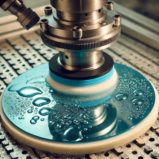
最も広く行われている調達エラーは、ステッカーの価格または「生のスループット」を比較することです。 ...収益性を実際に決定する数値は、ウェーハ 1 枚あたりのコストです...仕様 1 に合格するためのウェーハあたりの総コスト (機械の償却、消耗品、歩留まり損失)。精度の低い鋸は、たとえ安価で、より速く、スクラップ率が高くても、ウェーハ 1 枚あたりの価格が高くなります。.
作業例 ⁄ 良好なウェーハあたりのコスト
2 つのスライスセットアップが両方ともマシンタイムでウェーハあたり$2.00 プラス消耗品のコストがかかるとします:
- 82%ファーストパスでのレガシーソー歩留まり:$2.00 × 0.82 = よいウエファーごとの$2.44
- ダイヤモンドマルチワイヤーソー 96.5% 歩留まり: $2.00 × 0.965 = よいウエファーごとの$2.07
これは、余分なウェーハを数える前に、同じインゴットからより薄いカーフの勝利を得る前に、良好なウェーハあたりのコストが 15% 削減されます。独自のウェーハコストと測定された歩留まりを差し込んで、任意の 2 つのオプションを同様の基準で比較します。.
最良の価値オプション: 選択したオプションは、最高のROI、品質基準を満たすことを保証しながら、グッドウェーハあたりの最小有効コスト ーおよびプロセスツールでは、このプレミアムは、ドアから最高の品質、安全性 (UL、NFPA) 、およびウェーハを可能にしたときに、時間の経過とともに返済されます。 「グリッド: “構成の選択; “自宅での” スライス vs アウトソース」を参照してください”
| あなたの状態が...の場合 | 推奨方向 |
|---|---|
| 大容量、タイトなTTV、シリコン | 社内固定研磨ダイヤモンドマルチワイヤーソー; 取り扱いを自動化します |
| 低/可変容積、広い物質的な混合物 | 最初にスライシングをアウトソーシングします;資本の前に需要を検証します |
| 硬脆性化合物 (SiC、サファイア) | 材料一致ワイヤーspec +速度; 購入する前にテストカット |
| 超薄型ウェーハ (<100 μm) | 速度より振動制御+張力安定性を優先 |
莠 自家スライス ――利点
- 制御された TTV、トップサイド収量でのカーフ。.
- ボリュームに応じて優れたウェーハあたりのコストを削減します
- IPとプロセスレシピは内部に留まります
莠 社内スライス ――制限事項
- 資本支出とクリーンルームと計測
- 消耗品管理(配線が難しくなります)。.
- 訓練を受けたオペレーターとプロセスエンジニアリングが必要です
消耗品 “ハード真実” - a critical warning: wire is a consumable, not a fixture or part of your equipment kit in any way; a wire is consumed was the diamond wire during slicing, cutting force increases, leading to lower surface quality over a sliced segment/length, etc; 1 つは購入する必要がありますだけでなく、 a 精密 多 ダイヤモンド ワイヤー のこぎり, 、しかしまた1 つはウェーハの容積の切断を完了するために消費可能としてダイヤモンド ワイヤー自身を買います これを見ないバイヤーはよいウェーハごとの費用と著しく誤って述べます私達のダイヤモンド ワイヤー切断のベスト プラクティスのスライスを作ることの細部のROIの考慮のための記述を点検して下さい。.
つまり、コスト効率の高いツールは、優れたウェーハあたりのコストを最低にして、お客様のプロセス要件と品質と安全基準を満たしたツールです。高精度で高性能な機械は、その高性能によってプロセスの効率と再現性が向上し、十分な利益が得られる場合にのみプレミアムを獲得します。.
ウェーハ製造装置を作るのは誰ですか?段階的なベンダーの風景
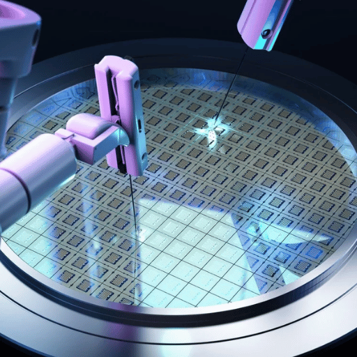
台湾積体電路製造公司のようなファブ向けのスライシングツールやベアウェハーを供給する単一のベンダーはなく、個々のベンダーがすべてのプロセスステップでエコシステム全体を支配しているわけでもありません。 むしろ、チップ製造内の各ニッチ市場には専門知識が必要なため、プロセスステップに従ってプロバイダーを分類することで、最も効果的なソリューション、たとえば「[すべての汎用サプライヤー] よりも優れたスライシング装置を製造しているのは誰ですか?」 に導きます?
- 結晶成長ベンダー: CZ またはフロート ゾーンを専門とし、ウェーハ用の単結晶インゴットを製造するクリスタル プラーおよび炉メーカー。.
- スライス装置ベンダー: ダイヤモンドマルチワイヤソー (MW) OEMメーカーでは、DONGHEのようなスライススペシャリストがしばしば利点を提供します。 「すべて」の広範なリストに対する精度が優れたTTV&カーフを提供することはここにあります。.
- 研削、ラッピング、エッジ準備機器のベンダー: 両面ラッパー;エッジグラインダー;ベベルマシン...
- ウェーハ研磨および化学機械平坦化 (CMP) 装置ベンダーおよび消耗品 (スラリー、パッド):... CMP スラリー メーカー.。.
- ウェーハ洗浄および計測ベンダー: シングルウェーハ クリーナー プロバイダーおよび Daitron Incorporated などの検査システムのスペシャリスト。.
各機器および消耗品のカテゴリー内で、サプライヤーは非常に狭いスペシャリストである場合もあれば、広範な機器メーカー (チップ製造会社にサービスを提供する統合機器ベンダー全体) である場合もあります。 - 世界中のチップメーカーは両方から購入しますが、「誰がウェーハを供給するか」、 - 裸のウェーハをファブに出荷する基板メーカー (GlobalWafers、信越、SUMCO (数量ベースの有名企業) など) - 製造部門と研究開発部門内で完全に別々に運営されています。彼らの研究開発プログラムはインゴット、プロセスに投資しており、このウェーハ加工およびスライス装置の購入者/顧客であり、その製造者や提供者ではありません。詳細については、当社のコンパニオンガイドをご覧ください 半導体ウェーハの種類 基板側を分解します 半導体製造装置 ガイドは回路ファブの半分をカバーします。.
チェーン全体にまたがるベンダーは存在しないため、購入者にとっての実際的な解決策は、測定された TTV とカーフでスライシングのスペシャリストを認定し、それを研磨と計測の別々のサプライヤーと統合することです。 DONGHE は、そのスライシング ステップを 6 μm 未満の TTV ターゲットに設計して提供します。この分野では、焦点を絞った OEM が広範なカタログを上回るパフォーマンスを発揮します。.
この風景を横断して、広範な半導体装置メーカーとシングルステップスペシャリストは、両方とも半導体生産に販売しています; グローバルウェーハのリーダーは、集中ベンダーが処理システムと半導体装置を供給しながら、製造施設を実行しても、最先端のウェーハ製造ラインはまだこれらの上流のスライシングおよび研磨ツールが提供するベアウェーハ品質に依存しています世界中の半導体メーカーからの需要は、両方を忙しくしています。.
SiC、サファイア、ソーラー: 複合基板装置がどのように異なるか
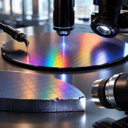
この点では、シリコンは、ダイヤモンド スライシング メーカーの新たなビジネスを促進する硬脆材料よりも準拠しています。 SiC、サファイア、および太陽電池グレードのシリコンは、それぞれ速度、張力、およびワイヤの寸法の変化を必要とします。なぜなら、材料の切除方法または除去方法がそれぞれ異なるからです。 SiC とサファイアはどちらも、それぞれの結晶構造の高い硬度と密度にはより高いワイヤ品質が必要であり、送り速度の低下によりデバイス効率が向上するため、シリコンとは異なり処理する先進的な材料です。.
そして、ほとんどのカタログに欠けている逆張りの考えがあります: 真実、ダイヤモンド線切断は、単結晶SiCウェーハであっても普遍的な万能薬ではないこと ー 特に、レーザーまたはコールドスプリットスライシングが実験作業中の既存のダイヤモンド線鋸では、それぞれ大きすぎ、薄すぎる直径とウェーハの厚さの範囲に適しています 「直径と基板に適した鋸を選択してください; シリコンプロセスの規模を想定しないでください」とサン氏は説明します。 SiC の硬度と強度により、ウェーハ研削とウェーハプロセスでのスラリー/CMP 化学の両方が再設計の義務を負っています。それが、今後のパワーデバイスランプが工場のバックエンドを再形成する原動力となります。.
涔️ 重要
非常に薄く、硬いウェーハは、スライス中にチップのはるかに簡単 ー 薄い半導体ウェーハをスライスすることの課題に関する論文では、シリコンの本質的な脆性からのチップ生成を重大なオープンチャレンジとして言及しています 約100 mのしきい値以下では、より高い処理速度を目指す代わりに、引張ひずみと振動の安定性を制御します。.
DONGHE の範囲はこれらの材料をカバーしています。専用資料を参照してください SiC ウエハ 切断 のこ そして サファイア 切断 ワイヤーソー 材料固有のパラメーターのページ、および基板自体の背景用の炭化ケイ素プライマー。.
ウェーハ製造装置の見通し:2026 年の需要を牽引するもの
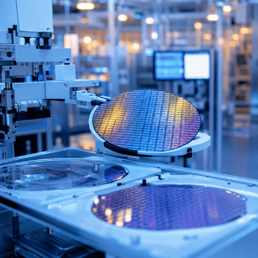
世界的な業界分析によると、シリコンウェーハ切断装置市場は2025年に$4.8Bに近く、2035年まで年間約7.4%で成長しているが、それを方向性背景としてのみ扱う。 2026年の購入者にとって、基本的な購入推進力はCAGRではない。重要なのは、購入者が建設中の容量と新しい容量が稼働する材料をどこに持つかということだ。.
私が目にする 2 つの傾向は次のとおりです。まず、ファブリショアリング - 米国が計画している米国本土でのチップ製造能力は、2022 年と比較して約 3 倍に近づき、約 25 の州地域で宣言された民間投資が $4,500 億近くに達する可能性があります。科学法。この新たな投資の一部は、新しいファブの近くにある新しい SiC エピタキシャルおよび基板の成長および製造施設に向けられています。標準化団体も同様に追いついています - SEMI はウェーハの定義を微調整しています。ただし、容積 450 mm は依然としてロットに滞留しています。.
シリコンへのさらなる取り組み パワーデバイス、家庭用電化製品、ディスプレイ (LCD) 、 集積回路 (IC) の消費者は、国内でより多くの半導体を構築している中国のチップメーカーで生産を増やしている。 「次世代ロジックチップ、新しいシリコンアーキテクチャ、より広いバンドギャップデバイスへのプッシュを控えてチップ技術が前進する中、既存のフロントエンド機器へのアクセスが依然として必要であると彼らは言う。現代のファブにおけるより多くの分析と新しいスラリー技術が証明しているように、チップ製造の世界では、限界は現在ウェーハ製造を超えていますが、インゴットからウェーハへのサプライチェーンの能力がそれらのチップに供給されています。.
購入者の行動: あなたの2026-2027 年のロードマップがパワーエレクトロニクスまたはホームサプライに触れている場合、あなたが過去にほんの数年を行う前に、事前に安全なスライス容量とワイヤー供給の精密ウェーハ製造装置のリードタイムは、地域全体が一度にファブを構築するときに長くなり、スライスステップ-あなたの収量上限-は、あなたがスポット可用性に残したくない1 つのダウンストリームの厚さの話をカバーしています ウエハ 薄化 ガイド.
容量を超えて、需要の増大と半導体技術のそれぞれの進歩 ―― 次世代ロジック、より広いバンドギャップ電力、新しい研究アプリケーション ―― 同じフロントエンドツールを活用し、最新のラインにより、高い歩留まり率の監視とより環境に優しいスラリー処理が追加されます。.
よくある質問frequently Asked Questions
Q: ウェーハ製造装置 (WFE) とは?
回答を見る
ウェーハ製造装置 (WFE) は、完成したシリコン ウェーハ上に集積回路を構築するツールのセットです (フォトリソグラフィー、エッチング、堆積および平面化 ⁄ 汚染管理されたクリーンルーム内)。これは、結晶成長、スライス、研削、研磨、洗浄など、裸のウェーハ自体を製造する初期の機械であるウェーハ製造装置とは異なります。.
2 つのツールラインは、ほぼ完全に異なる顧客にサービスを提供するため、この区別は、バイヤーにとって重要です ウェーハハウスは、クリスタルプラー、スライシングソー、グラインダー、研磨機を購入する一方、回路ファブはリソグラフィー、エッチング、蒸着に投資します これらの用語は会話の中で同じ意味で使用されることが多いため、比較する前に、必ず見積書がプロセスのどの部分をカバーしているかを確認してください。.
Q: インゴットからシリコンウェーハはどのようにスライスされますか?
回答を見る
ダイヤモンドマルチワイヤソーは、インゴット全体を 1 回のパスでウェーハのフルセットに切断します。ダイヤモンド埋め込みワイヤ 1 本に、平行な溝を何百回も通します。そのカーフは、およそ 70 ~ 150 マイクロメートルで、古いスラリーマルチワイヤソーの 180 ~ 220 マイクロメートルよりもはるかに少ないシリコンを無駄にします。.
この細かい縁石は、全体の厚さの変動が小さくなり、表面の汚染も少なくなります。 1 つすべてが下流に持ち上げられます。.
Q: TSMCのような企業にシリコンウェーハやウェーハ装置を供給しているのは誰ですか?
回答を見る
ベアシリコンウェーハは、市場シェアをリードするglobalwafers、信越、sumcoなどの基板メーカーから提供されています。これらのウェーハメーカーは、上流ツーリングのサプライヤーではなく、顧客です。そのウェーハ装置は、水晶引き OEM、ダイヤモンドワイヤースライサーメーカー、エッジグラインダー、研磨機、洗浄ツール、さらに測定および検査ベンダーなど、機能別に組織された専門家によって提供されます。.
ウェーハ作成ライン全体をカバーするプロバイダーは 1 つではないため、スライシングのようなメイク オア ブレーク ステップに焦点を当てたスペシャリストは、最終的により良い結果をもたらすことができます。そのため、「巨大なチップ生地にウェーハを供給する人」は、「ウェーハ切断鋸を供給する人」と同じ問題ではありません“
Q: TTVは何を意味し、なぜそれが重要ですか?
回答を見る
これは、総厚さ変動 (TTV) - 特定のウェーハ上の最も厚い寸法と最も薄い寸法の区別を表します。 TTV は、リソグラフィーの正確な焦点面にとって重大な問題です。ウェーハの幅が全体的に変化しすぎると、レンズが正確に焦点を合わせることができなくなり、ウェーハ上の要素が正確に焦点を合わせることができなくなり、金型が降伏することを示唆しています。総厚さ変動はスライスを開始し、研削や研磨中に単純に多少平滑化されるだけになる場合があります。つまり、鋸が最終的な製造を真に決定することを意味します。.
Q: ウエハ製造設備はいくらですか?
回答を見る
これは、プロセスの段階、ウェーハの寸法、自動化の程度によって異なります; そしてこれは、任意の1 つの統計が誤解を招くことを意味し、その代替として、完成したウェーハあたりのコストに集中し、主題を使用してチェックスライスを要求します。.
Q: 今日生産で最大のウェーハサイズは何ですか?
回答を見る
現在、大量生産は 300 mm のシリコン ウェーハで実行されており、ロジックとメモリのスライスを支配しています。 450 mm フォーマットは何年も前に定義されましたが、ツーリングの経済性が法外に高価であることが判明したため、量産には至りませんでした。 SiC やサファイアなどの複合基板の場合、これらのラインがスケールアップしても 150 mm と 200 mm が動作サイズのままです。.
この分析について
このガイドのスライシング仕様とSiliconTechの歩留まり数値は、DONGHEが独自にインゴット-ウェーハチェーンのスライシングステーションにダイヤモンドマルチワイヤソーを現場展開し、査読済みのダイヤモンドワイヤソーの文献とSEMI M1 ウェーハ仕様と照合して、ここで説明する歩留まり上限を設定するワイヤソーを構築するため、コストパーグッドウェーハビューは実際のラインで測定したものを反映しています。 Shanghai Donghe Science and Technology Co., Ltd.の技術チームによってレビューされました。.
参考文献と情報源
- シリコンウェーハ製造プロセスBYU クリーンルーム (ブリガム ヤング大学)
- ダイヤモンドワイヤーソーンシリコンにおける地下マイクロクラック損傷深さの予測PMC / 米国国立医学図書館 (Wang et al., 2024)
- シリコンウェーハの表面形態および表面下の損傷に対するダイヤモンドワイヤー摩耗の影響ScienceDirect (Kumar et al., 2016)
- 薄型半導体ウェーハのスライスにおける進歩と重大な課題ストラスクライド大学 / 半導体処理における材料科学 (2025)
- シリコン材料の特性評価の進化 (弓/経糸、SEMI 参照)NIST
- 450mm規格の更新 (SEMI M1-0114)半導体エンジニアリング
- 米国半導体産業の現状 (CHIPS 法による容量)半導体 産業 協会 (SIA)
- US8256407B2、マルチワイヤソーおよびインゴット切断方法(張力制御)Google特許経由のUSPTO
![ポリシリコン素材:特性、グレード、用途 [ガイド]](https://wiresawcutter.com/wp-content/uploads/2026/08/polysilicon-material-featured-768x512.webp "ポリシリコン材料: 太陽光および半導体産業における特性、グレードおよび用途 12")

![ポリシリコン素材:特性、グレード、用途 [ガイド]](https://wiresawcutter.com/wp-content/uploads/2026/08/polysilicon-material-featured-150x150.webp)