DONGHE Company に連絡してください

シリコンウェーハ材料は、携帯電話のプロセッサから電気自動車のパワーモジュールに至るまで、ほぼすべての半導体デバイスが構築されている薄くて超純粋な結晶ディスクです。しかし、ほとんどの説明は「砂から作られている」ということで終わります。しかし、ウェーハを指定したり、購入したり、スライスしたりするときに実際に重要な部品、つまりどの結晶タイプを選択するか、どの厚さと平坦性が期待できるか、インゴットが何百ものミラーフラットディスクになるか、そして途中にどれくらいのコストのシリコンが塵として消えるかはスキップします。.
このガイドでは、実数と基準を背後に付けて、そのすべてを説明します。私たちは、硬くて脆い材料用の切断装置を構築するため、百科事典的なガイドが覆い隠している 1 つの段階、つまり、すべてのインゴットの驚くべき割合が失われるスライス ステップに特に注意を払います。のこぎり。.
クイックスペック: 一目でわかるシリコンウェーハ材質
| ベース材質 | 電子級シリコン(EGS)、純度99.9999999%+(9N ~ 11N) |
| 結晶構造 | 単結晶 (CZ またはフロートゾーン) または多結晶 |
| 一般的な直径 | 100、150、200、300 mm (450 mm はまだ量産前) |
| 標準厚さ | SEMI M1 あたり約 525 μm (100 mm) ~約 775 μm (300 mm) |
| 一次ドーパント | ホウ素(p型)、リン(n型) |
| 主な用途 | 集積回路、パワーデバイス、太陽電池、MEMS、センサー |
シリコンウェーハとは何ですか?

シリコンウェハーは、電子部品を構築するための基板、つまり基礎として機能する単一のシリコン結晶の薄いスライスです。エレクトロニクスでは、a ウェーハは半導体の薄いスライスです トランジスタ、ダイオード、および相互接続が層ごとに製造される上およびその内部。ウェーハ自体は、処理されるまで電気的にほとんど何も行いません。その仕事は、数十億のデバイスを表面全体にパターン化できるように、原子レベルで平坦でクリーンで完全に順序付けされることです。.
シリコンがこの役割を獲得したのは、次の 3 つの理由からです。シリコンは豊富に存在すること、優れた絶縁体を作る安定した天然酸化物 (二酸化シリコン) を形成すること、そして他の元素を微量に添加することでその電気的挙動を正確に調整できること。 300 mm のウェーハ 1 枚で数千個のチップを搭載でき、それぞれが数十億個のトランジスタを保持していること。そのスケールが、ウェーハがチップ製造における通貨の単位である理由です。fabs は、チップではなく「ウェーハが 1 か月あたりに開始する」という出力を測定します。.
💡 キーテイクアウェイ
ウェーハは完成したデバイスではなく基板です。その価値は平坦度、純度、結晶の秩序から生まれます ¢ 後の処理ステップごとに 3 つの特性が依存します。.
シリコンウェーハは何で作られていますか?

シリコンウェーハは、地球上で最も純粋な工業用材料の1 つである電子グレードのシリコンから作られています その旅は、通常の珪砂 (二酸化シリコン) から始まり、アーク炉で約98 ~ 99%純度で冶金グレードのシリコンに還元される、エレクトロニクスには十分とは言えないため、シリコンはガス (トリクロロシラン) に変換され、蒸留され、シーメンスプロセスを通じて固体ポリシリコンとして再び堆積されます その堆積されたポリシリコンは、99.9999999%純度以上、9 から11 の「9」に達します“
シリコンウェーハは正確には何でできていますか?
ウェーハの段階では、材料はほぼ純粋なシリコンプラス意図的な、微量のドーパントです 純度を大局的に言うと: 9Nシリコンは、シリコン原子10 億個あたりおよそ1 個の異物原子を許可します そのドーパント、通常 ホウ素 p型の場合または リン n-type の場合、結晶成長中に意図的に、10 億分の 1 から 100 万分の 1 で測定される濃度で添加されます。これらの微量原子がシリコンに有用な半導体挙動を与えるものです。それらがなければ、超純シリコンは室温で絶縁体に近くなります。砂は世界中に豊富にありますが、精製、結晶成長、スライスによって、完成したウェーハが高価になるのは生のシリコンではなく、です。.
シリコンウェーハの種類: 単結晶対多結晶

シリコンウェーハは、結晶構造とその加工方法に基づいていくつかのファミリーに分類されます。最も重要な分割は単結晶と多結晶ですが、SOI やエピタキシャルウェーハなどの人工基板も重要です。.
| タイプ | 結晶構造 | 代表的な用途 | 相対コスト |
|---|---|---|---|
| 単結晶 (CZ) | 単連続結晶 | IC、ロジック、メモリ、ほとんどのチップ | 高い |
| 単結晶 (フロートゾーン) | 単結晶、より高い純度 | 電源装置、検出器、高効率ソーラー | 最高 |
| 多結晶 | 多くの穀物、目に見える微結晶 | 低コストの太陽電池 | ロウ |
| SOI (シリコンオンインシュレータ) | シリコン/酸化物/シリコンスタック | RF、低電力、自動車用チップ | プレミアム |
| エピタキシャル | ベースウエハー上に成長したクリスタル層 | 電源、アナログ、CMOS イメージ センサー | プレミアム |
シリコンウェハーの3 種類とは?
人々が「3 つのタイプ」を求めるとき、彼らは通常、3 つの結晶形を意味します: 単結晶 (1 つの連続した水晶、ほとんどすべての集積回路のために使用される)、, 多結晶/多結晶 (多くの小さな穀物、予算のソーラーパネルで一般的)、および 非晶質 シリコン (長距離注文なし、薄膜セルや一部のディスプレイで使用) ドーピングは2 番目の軸を追加します: これらのいずれかをホウ素でp型にしたり、リンでn型にしたりできます 頻繁かつコストのかかる混在の1 つは、多結晶太陽シリコンをICグレードの単結晶と交換可能として扱うことであり、それらは異なる純度レベルと非常に異なる価格帯に位置し、それらは代替品ではありません。.
シリコンウェーハのサイズ、厚さ、仕様

ウェーハの寸法は任意ではありません。 SEMI 規格 (主に SEMI M1) に準拠しているため、どこにでも作られたファブ機器はどこでも作られたウェーハを処理できます。直径が大きくなるにつれて、厚さも大きくなります。これは、ディスクが大きいほど、ひび割れやたるみなく取り扱いを生き残るために、より多くの機械的剛性が必要であるためです。.
| 直径 | 公称厚さ | 共通エッジ機能 |
|---|---|---|
| 100 のmm (4 の″) | ~525μm | 一次アパート + 二次アパート |
| 150 のmm (6 の″) | ~625~675μm | フラッツ |
| 200 のmm (8 の″) | ~725μm | ノッチ |
| 300 のmm (12 の″) | ~775μm | ノッチ |
直径と厚さを超えると、3 つの平坦度パラメータが仕様シート上でほとんどのことを行います。. TTV (総厚さの変化) は、ウェーハ全体の最も厚い点と最も薄い点の差です。. ボウ 中心が基準面からどれだけ逸脱しているかを測定します ワープ 中央面のピークから谷への完全なたわみを捉えます。ドーパント濃度によって設定される抵抗率は、コアの電気仕様を丸くします。最先端のリソグラフィーの場合、300 mm ディスク全体のサブミクロンの平坦性はそれほど良くありません。これは、鮮明な印刷パターンとウェーハ エッジの焦点の合っていないパターンの違いです。.
嬴工注
最終的なウェーハの平坦度はスライスステップで上限が設定されます。 low TTVで指定された300 mmのウェーハは、鋸が波状の表面を残した場合、研磨だけでは救助できず、ラッピングと研磨で数ミクロンしか除去できません。そのため、TTVをスライスすると、研磨品質だけでなく、現実的な平坦度予算が設定されます。ノコギリが保持できるスライスされたままのTTVの周りに、厚さ許容量(通常はラッピング/エッチング/研磨用の数十ミクロンのストック)を計画します。.
シリコンウェーハの作り方: 砂からインゴットまで

ウェーハ製造は精製されたポリシリコンを完成したディスクに変え、それは単結晶を成長させることから始まります。 2つの主要な方法があり、その選択は純度と価格に実際の結果をもたらします。.
の The チョクラルスキー (CZ) プロセス 石英るつぼ内のポリシリコンを溶かし、種結晶を溶融物に浸し、ゆっくりと上に引っ張って回転させて、種子から単結晶が下方に成長します。 CZ は、ボリュームチップ製造に必要な大口径のインゴットを生成し、ほとんどの市販のウェーハの主力製品です。そのトレードオフ: 石英るつぼは結晶に酸素を導入するため、抵抗率が制限されます。.
フロートゾーン方式ではるつぼを完全にスキップします。ポリシリコンロッドは、表面張力によって所定の位置に保持された狭い移動ゾーンで溶融され、ゾーンが移動するにつれて不純物が掃引されます。その見返りは並外れた純度です。. フロートゾーンシリコン CZが一致するのに苦労する抵抗率と純度レベルに達する、それがパワーデバイスと放射線検出器のために選択される理由 これはまた、一般的な仮定が壊れる場所: 安いのは常に太陽のための規則に関する研究 太陽電池用フロートゾーンシリコン は、25%付近でのセル効率を実証している ⁄ 最も安価なシリコンではなく、最も純粋なシリコンが性能の上限を設定する証拠 結晶成長がより広い人々にどのように供給するかについての背景について 太陽光発電のサプライチェーン, 、米国エネルギー省は有用な概要を維持している。 のこの図解ウォークスルーを段階的に説明すると、 チョクラルスキー結晶成長法.
インゴットが成長したら、その端を切り取り、シリンダーを正確な直径に研磨し、結晶の向きを示すためにノッチまたはフラットを加工します。そうして初めて、スライスする準備が整います。次に掘り下げるステップです。.
スライスとウェハリング: インゴットがウェハーになる方法

スライスとは、長さ 1 メートルのシリコン インゴットが数百枚の個別のウェーハになり、驚くべき量の高価な材料が消える場所です。現代の工場や太陽光発電会社は、ダイヤモンド ワイヤー ソーでインゴットをスライスします。これは、細かいダイヤモンド グリットでコーティングされた 1 本の鋼線で、数百本の平行なパスのウェブにねじ込まれ、インゴット全体が一度に切断されます。.
カーフ税: すべてのインゴットの大部分がウェーハにならない理由
これは「砂からチップへ」のストーリーがスキップする部分です。すべてのカットには幅があり、カーフがあり、そのカーフ内のすべてのシリコンは塵に変わります。歴史的に、スライスではインゴットの 40% 程度が失われ、損傷が見られ、高価な超純結晶の大部分が使用可能なウェーハとして出荷されることはありません。薄い太陽光発電ウェーハでは計算が過酷です。ウェーハの厚さがおよそ 150 ~ 180 μm で、鋸の縁石がそのかなりの部分である場合、カットに失うシリコンは維持する限りほぼ同量になります。研磨ではなくスライスすることで、インゴットがどれだけのウェーハを生成するかが決まることがよくあります。.
これはまさに業界が古いスラリーソーからダイヤモンドワイヤーに移行した理由です スラリーソーイングは約200 ~ 250 µmの縁石の幅を残しました; 現代 シリコンウェーハ切断用ダイヤモンドワイヤソー それをおよそ60 ~ 80 µmまで下げて、より速く走らせ、研磨スラリーを完全にスキップします。 の学術的レビュー 薄い半導体ウェーハのスライス (Mechanical Systems and Signal Processing、2025) 同じ結論に達します。ウェーハの厚さとワイヤの直径の両方を減らすことが、パスごとに失うカーフを縮小するため、歩留まりを高めるための最も効果的な手段です。.
嬴工注
ワイヤー直径、送り速度、ワイヤー張力が一緒になってカーフロスとスライスされたままの TTV の両方を設定します。ワイヤーが細かくなるとシリコンは節約されますが、たわみや破損が発生しやすくなるため、カットパラメーターは単一の「最良」数値ではなくバランスになります。脆くて価値の高い結晶の場合、狭いカーフでタイトな TTV を保持する鋸は、材料が保存された状態と、完成したウェーハに生き残る平坦性の状態の両方で 2 回降伏を保護します。.
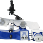
同じスライシングの物理が、硬くて脆い材料、サファイア、炭化ケイ素、結晶性シリコン全体に適用され、ワイヤーソーの下ではすべて同じように動作します。そのため 硬くて脆い材料の切断 は一つの工学分野として扱われ、その理由 精密ダイヤモンド ワイヤー鋸システム 素材ごとに調整されています.
ウェーハグレードと品質パラメータ

すべてのアプリケーションが完璧なウェーハを必要とするわけではなく、そうでないときにウェーハの代金を支払うことは静かな予算漏れです。ウェーハは、表面品質と価格を交換するグレードで販売されています。.
| グレード | 品質 | のためのベスト |
|---|---|---|
| プライム | デバイス品質;最もきつい平坦性、最も低い欠陥 | 生産用ICおよびデバイス |
| テスト | わずかに低い表面品質; わずかな化粧品の欠陥、まだ機能的 | プロセス開発、R & D |
| ダミー/モニター | デバイスグレードではなく、機械/プロセスプレースホルダー | ツールのチューニング、ハンドリングテスト |
| 奪還する | 再調整/剥がし、再研磨 | コスト重視のモニターとテスト実行 |
エンジニアは、重要でない作業のためにプライムグレードのウェーハを頻繁に過剰に指定し、デバイスグレードの価格を支払って、テストまたは再生ウェーハが問題なく処理するプロセスを調整します。 1 つの簡単なルールが役立ちます: ウェーハが出荷されたデバイスになる場合は、プライムを購入します; そこに向かう途中でステップである場合、通常は低いグレードが作業を行います。. 再生ウェーハ、以前の層を剥ぎ取り、表面を再研磨したプライムまたはテストウェーハは、製品に影響を与えることなくファブコストを抑制できるため、モニターウェーハとして広く再利用されています。グレードを分ける品質指標は、仕様書と同じです: TTV、弓、縦糸、粒子数、抵抗率許容値。.
シリコン vs. SiC vs. GaN: ウェーハ材料の選択

シリコンは体積で支配的ですが、ウェーハ材料はシリコンだけではなく、一部のジョブではウェーハ材料が間違っています。ピックを決定するのは通常、バンドギャップです。バンドギャップは、材料が半導体のように動作しなくなるまでにかかる電圧と熱の量を設定します。.
| 材料 | バンドギャップ | 際立つ物件 | ベストフィット |
|---|---|---|---|
| シリコン (Si) | ~1.1 eV (間接) | 安価で、豊富で、成熟したプロセス | 論理、メモリ、ほとんどのチップ |
| 炭化ケイ素(SiC) | ~3.3 eV(ワイド) | 高電圧、高温、高い熱伝導率 | EVインバータ、パワーエレクトロニクス |
| 窒化ガリウム (GaN) | ~3.4 eV(ワイド) | 高速スイッチング、高周波 | 充電器、RF、電力変換 |
| ガリウムヒ素 (GaAs) | ~1.42 eV(ダイレクト) | 高い電子移動度、発光 | RF、マイクロ波、LED/レーザー |
| リン化インジウム (InP) | ~1.34 eV(ダイレクト) | 赤外線光学 | 光ファイバー、フォトニクス |
禹 なぜシリコンはまだほとんどの仕事を獲得します
- 規模に応じてエリアあたりのコストが最も低くなります
- 数十年にわたる成熟したファブプロセス
- ネイティブ酸化物は絶縁を容易にします
- 処理中~1,400° Cまで安定
広帯域ギャップが勝つ場合
- シリコンの限界を超える高電圧電力 (SiC)
- 高周波スイッチング (GaN)
- 熱処理が向上し、システムが小型化されます
- 材料とスライスのコストが高くなります
クイック決定ルール: 一般的なロジックとメモリの場合、シリコンがデフォルトです。高電圧電力変換、EV ドライブトレイン、産業用インバーターの場合炭化 ケイ素 ウエハ 切断 のこぎり 効率と熱でテリトリーが勝利します。 急速充電器とRFの場合、GaN。 SiCを具体的に計量している場合は、当社のより深い 材料としての炭化ケイ素のガイド ポリタイプと特性を詳細にカバーします これらの広帯域ギャップ結晶はシリコンよりもさらに硬く脆いため、切断のようにスライスします ワイヤーソー付きサファイアワイヤーとフィードのより厳格な制御が必要です。.
シリコンウェーハの用途

シリコンウェハは、ウェハ製造を通過すると、ほぼすべての電子システムに行き着きます。その使用範囲は、簡単に過小評価できます:
- ✔ ロジックおよびメモリ ICマイクロプロセッサとDRAM/フラッシュ、1 つのダイに数十億個のトランジスタを保持できる。 the マイクロプロセッサ はマーキーの例である.
- ✔ パワーデバイス電話充電器からグリッドインバーターに至るまで、あらゆる機器の電気を管理するダイオード、MOSFET、IGBT.
- ✔ 太陽電池太陽光発電ウェーハは太陽光を直接電気に変換し、世界のウェーハ面積の大きなシェアを占めています。.
- ✔ MEMS とセンサー加速度計、圧力センサー、マイクロホンをシリコンに直接エッチングします。.
- ✔ イメージセンサーとフォトニクス光データ用のCMOSカメラセンサーとシリコン導波路。.
太陽光発電は、ウェーハ面積の使用量がこれまでで最も多く、最も縁石に敏感であるため、特筆する価値があります。そのため、太陽光発電メーカーは、最初にダイヤモンドワイヤーとより薄いウェーハを押して、専用のようにPVレンガをスライスする装置 ソーラーパネル切断機, 、シリコン各キログラムからより多くのウエハを絞ることを中心に設計されています。.
業界の見通し: 2026 年のシリコン ウェーハ材料

ウェーハ市場は爆発的ではなく着実に成長しています。 推定値は範囲によって異なりますが、 フォーチュン ビジネス インサイト シリコンウェーハ市場は2025年に約$114億、2026年には約$121億に上昇すると推定します。. BCC リサーチ より広範な半導体シリコンウェーハセグメントを、$138億ベースから$202億ベース、つまり2030年までの年間レート約6.7%に向けて追跡します。これらの数値は、範囲が異なるため異なりますが、方向性は一貫しています。つまり、一桁の需要主導の成長です。.
2026 年中に3 つのシフトを計画する価値があります まず、, 300mmの圧密化も続くAIアクセラレータ、自動車用エレクトロニクス、エッジコンピューティングによって駆動され、450 mmはプリプロダクションで失速したままです。 2つ目は、, 広帯域ギャップ材料はシリコンよりも速く成長しています; 特にSiCウェハの需要は、シリコンがボリュームバックボーンのままであるにもかかわらず、EVおよび電力アプリケーションの規模拡大に伴い、年率2 桁で拡大しています 第3 に、, スライスは無駄を省き続けます: より薄いウェーハとより細いダイヤモンド ワイヤーは、前述の縁石損失を削減するための主な手段であり、その傾向はまさに利回りの経済性に関するものです。.
2026 年のプロジェクトのウェーハまたは容量を指定する場合、実際的な動きは、シリコンの体積作業に 300 mm を想定し、設計が電力または RF 負荷が大きい場合は SiC または GaN に個別に予算を立て、スライス収量をラインとして扱うことです。今日のシリコン価格ではカーフはリアルマネーであるため、後付けではなく項目です。.
よくある質問frequently Asked Questions
Q: なぜシリコンウェーハはこんなに高価なのか?
回答を見る
それは砂ではありません。コストは、シリコンを純度 9 ~ 11 ナインに精製すること、エネルギーを大量に消費する結晶の成長、ゆっくりとしたスライスステップ (結晶の大部分がカーフとして失われる)、およびサブミクロンの平坦性を達成するために必要なラッピング、エッチング、研磨から発生します。厳しい欠陥と抵抗率の許容差がそれをさらに促進します。原材料は安いです。精度はあなたが支払うものです。.
Q: どの国がケイ素のウエハーの供給を導きますか?
回答を見る
ポリシリコンと生のシリコン生産は中国に集中している一方、日本(信越やSUMCOなど)、台湾(グローバルウェーハ)、ドイツの少数の企業が完成したプライムウェーハ供給を支配している。市場は異常に集中している。世界のハイエンドの300mmウェーハをほとんど製造している企業は一握りであり、各工場は生産前の数か月間、独自のプロセスに対してウェーハを適格にするため、サプライヤーの切り替えが遅い。その集中と、新たな生産能力を構築するための複数年にわたるリードタイムが組み合わさって、ウェーハ供給の安全性が産業政策に現れ続け、買い手が現地を購入するのではなく長期的な数量契約に署名することが増えている理由である。.
Q: 一般的なシリコンウェーハの厚さはどれくらいですか?
回答を見る
厚さは直径に応じてスケールします。 100 mm のウェーハは約 525 μm、200 mm は約 725 μm、300 mm は約 775 μm です。積み重ねられたデバイスやフレキシブルデバイス用の特殊な薄型ウェーハは 100 μm をはるかに下回る可能性がありますが、壊れやすいため、特別な取り扱いが必要です。.
Q: シリコンウェーハは再生または再利用できますか?
回答を見る
はい。 primeまたはテスト ウェーハを使用した場合、表面層を剥がして再生ウェーハに再研磨し、工具の校正やプロセス チェック用のモニターまたはダミー ウェーハとして再利用できます。これは、ファブにおける標準的なコスト管理手法であり、実際の製品ウェーハには触れません。.
Q: 生産で最大のシリコンウェーハサイズは何ですか?
回答を見る
300 mm (12 インチ) がボリュームの標準です。 450 mm の移行は機器のコストと欠陥制御で停止しているため、2026 年の実用的な上限は 300 mm です。.
Q: インゴットからシリコンウェーハはどのようにカットされますか?
回答を見る
ダイヤモンドワイヤーソーは、ダイヤモンドグリットでコーティングされた平行ワイヤーパスのウェブを使用してインゴット全体を一度にスライスします。これは、より狭い縁石を切断し(200~250μmに対して約60~80μm)、より速く走り、シリコンの無駄が少ないため、古いスラリーソーイングに取って代わりました。スライス後、ウェーハは端を研磨し、ラップし、エッチングし、最終仕上げまで研磨します。.
硬くて脆い結晶をスライスしますか?
カーフ損失とスライスされたままの平坦性がウェーハの歩留まりを決定します。専用のダイヤモンド ワイヤー ソーが、より狭いカーフとよりきつい TTV でシリコン、SiC、サファイアをどのように切断するかを確認してください。.
このガイドを書いた理由
当社は、シリコン、炭化ケイ素、サファイアを切断するためのダイヤモンド ワイヤー ソーを設計および構築しているため、ほとんどのウェーハ概要で除外されているカーフ損失を含む、スライシングのステップを間近で見ることができます。ここでの厚さ、グレード、バンドギャップの数値は、SEMI 標準、ウェーハ スライシングに関する出版された学術研究、および名前付き市場調査ソースから抽出されたものであり、ベンダーのマーケティング主張は意図的に引用から除外されています。.
参考文献と情報源
- ウェーハ (電子機器)ウィキペディア
- チョクラルスキープロセスウィキペディア
- フロートゾーンシリコンウィキペディア
- 太陽電池の大量生産用のフロートゾーンシリコンハーバード ADS (学術記録)
- 薄型半導体ウェーハのスライスにおける進歩と重大な課題 (MSSP、2025)ストラスクライド大学 (ストラスプリント)
- 太陽光発電の基礎米国 エネルギー省
- チョクラルスキーシリコン(PVCDROM)PVEducation (アリゾナ州立大学)
- マイクロプロセッサブリタニカ百科事典
- シリコンウェーハの市場規模と見通しフォーチュン ビジネス インサイト
- 半導体 シリコンウェハ 市場BCC リサーチ
- SEMI M1、研磨単結晶シリコンウェーハの仕様 (SEMI 国際規格)


 的 (なな) 的 (て) 的 (て) な (な) もの (な) もの (な) もの (な) もの (な) もの (な) もの (な) もの (な) もの (な) もの (な) もの (な) もの (な) もの (な) もの (な) もの (な) もの (な) もの (な))
