Nehmen Sie Kontakt mit DONGHE Company auf

Siliziumwafermaterial ist die dünne, ultrareine kristalline Scheibe, auf der fast jedes Halbleitergerät aufgebaut ist, vom Prozessor in Ihrem Telefon bis zum Leistungsmodul in einem Elektroauto. Die meisten Erklärungen enden jedoch bei “es besteht aus Sand”” Das stimmt, aber es überspringt die Teile, die tatsächlich wichtig sind, wenn Sie Wafer spezifizieren, kaufen oder schneiden: welche Kristallart Sie auswählen, welche Dicke und Ebenheit Sie erwarten können, wie aus einem Barren Hunderte von Spiegelscheiben werden und wie viel kostspieliges Silizium verschwindet unterwegs als Staub.
Dieser Guide geht durch all das, mit reellen Zahlen und den dahinter stehenden Standards Wir bauen Schneidgeräte für harte, spröde Materialien, deshalb achten wir besonders auf eine Stufe, die die enzyklopädischen Guides beschönigen: den Schneidschritt, bei dem ein überraschender Anteil jedes Barrens an der Säge verloren geht.
Schnelle Spezifikationen: Siliziumwafermaterial auf einen Blick
| Grundmaterial | Silizium in elektronischer Qualität (EGS), Reinheit 99,9999999%+ (9 N 11 N) |
| Kristallstruktur | Monokristallin (CZ oder Float-Zone) oder multikristallin |
| Übliche Durchmesser | 100, 150, 200, 300 mm (450 mm noch Vorproduktion) |
| Standarddicke | ~525 µm (100 mm) bis ~775 µm (300 mm), pro SEMI M1 |
| Primärdopanten | Bor (p-Typ), Phosphor (n-Typ) |
| Hauptverwendungen | Integrierte Schaltkreise, Energiegeräte, Solarzellen, MEMS, Sensoren |
Was ist ein Siliziumwafer?

Ein Siliziumwafer ist eine dünne Scheibe eines einzelnen Siliziumkristalls, die als Substrat, als Fundament, für den Aufbau elektronischer Bauteile dient In der Elektronik ist ein Wafer ist eine dünne Halbleiterscheibe Auf und innerhalb derer Transistoren, Dioden und Verbindungen Schicht für Schicht hergestellt werden Der Wafer selbst macht fast nichts elektrisch, bis er verarbeitet ist; Seine Aufgabe besteht darin, flach, sauber und perfekt auf atomarer Ebene geordnet zu sein, damit Milliarden von Geräten über seine Oberfläche strukturiert werden können.
Silizium hat sich diese Rolle aus drei Gründen verdient: Es ist reichlich vorhanden, es bildet ein stabiles natives Oxid (Siliziumdioxid), das einen hervorragenden Isolator darstellt, und sein elektrisches Verhalten kann durch Zugabe winziger Mengen anderer Elemente präzise abgestimmt werden Ein einzelner 300-mm-Wafer kann Tausende einzelner Chips tragen, von denen jeder Milliarden von Transistoren enthält. Deshalb ist der Wafer die Währungseinheit bei der Chipherstellung. Fabs messen die Produktion in “Waferstarts pro Monat”nicht in Chips.
💡 Schlüssel zum Mitnehmen
Der Wafer ist ein fertiges Gerät, kein fertiges Gerät Sein Wert kommt von der Ebenheit, Reinheit der Kristallordnung, und die Eigenschaften der Kristalle hängen von jedem späteren Verarbeitungsschritt ab.
Woraus bestehen Siliziumwafer?

Siliziumwafer werden aus Silizium in elektronischer Qualität hergestellt, einem der reinsten Industriematerialien der Erde. Seine Reise beginnt mit gewöhnlichem Quarzsand (Siliziumdioxid), der in einem Lichtbogenofen auf Silizium in metallurgischer Qualität mit einer Reinheit von etwa 989991TP3 T reduziert wird, das ist bei weitem nicht gut genug für die Elektronik, daher wird das Silizium in ein Gas (Trichlorsilan) umgewandelt, destilliert und durch den Siemens-Prozess als festes Polysilizium zurückgeschieden Das abgeschiedene Polysilizium erreicht eine Reinheit von 99999991TP3 T oder besser neun bis elf “Ninen”
Woraus bestehen Siliziumwafer, genau?
Im Waferstadium ist das Material nahezu reines Silizium plus absichtliche, Spurenmengen eines Dotierstoffs Um die Reinheit ins rechte Licht zu rücken: 9 N Silizium erlaubt ungefähr ein Fremdatom pro Milliarde SiliziumatomeDieses Dotierstoff, normalerweise Bor Für p-Typ bzw Phosphor Für n-Typ, wird absichtlich während des Kristallwachstums hinzugefügt, bei Konzentrationen, die in Teilen pro Milliarde bis Teilen pro Million gemessen werden Diese Spurenatome sind es, die dem Silizium sein nützliches halbleitendes Verhalten verleihen; ohne sie ist ultrareines Silizium bei Raumtemperatur nahe an einem Isolator Sand ist weltweit reichlich vorhanden, aber die Raffination, das Kristallwachstum und das Schneiden sind es, die einen fertigen Wafer teuer machen, nicht das rohe Silizium.
Arten von Siliziumwafern: Monokristallin vs. Polykristallin

Siliziumwafer lassen sich je nach Kristallstruktur und Verarbeitung in einige Familien einteilen. Die wichtigste Spaltung ist monokristallin versus multikristallin, aber auch technische Substrate wie SOI und epitaktische Wafer sind wichtig.
| Typ | Kristallstruktur | Typische Verwendung | Relative Kosten |
|---|---|---|---|
| Monokristallin (CZ) | Einstetiger Kristall | ICs, Logik, Speicher, die meisten Chips | Hoch |
| Monokristallin (Schwimmzone) | Einkristall, höhere Reinheit | Energiegeräte, Detektoren, hocheffiziente Solaranlage | Höchste |
| Multikristallin | Viele Körner, sichtbare Kristallite | Kostengünstigere Solarzellen | Niedrig |
| SOI (Silizium-auf-Isolator) | Silizium/Oxid/Siliziumstapel | HF, Low-Power, Automobilchips | Premium |
| Epitaxial | Gezüchtete Kristallschicht auf einem Basiswafer | Leistungs, analoge, CMOS-Bildsensoren | Premium |
Was sind die drei Arten von Siliziumwafern?
Wenn Menschen nach “drei Typen” fragen, meinen sie normalerweise die drei Kristallformen: Monokristallin (ein kontinuierlicher Kristall, der für fast alle integrierten Schaltkreise verwendet wird), Polykristallin / multikristallin (viele kleine Körner, die in preisgünstigen Solarmodulen üblich sind) und Amorph Silicium (keine Fernordnung, in Dünnschichtzellen und einigen Displays verwendet) Dotierung fügt eine zweite Achse hinzu: jede davon kann mit Bor p-Typ oder n-Typ mit Phosphor gemacht werden Eine häufige und kostspielige Verwechslung ist die Behandlung von multikristallinem Solarsilicium als austauschbar mit monokristallinem IC-Grad, sie sitzen auf unterschiedlichen Reinheitsgraden und sehr unterschiedlichen Preispunkten, und sie sind keine Ersatzstoffe.
Siliziumwafergrößen, -dicke und -spezifikationen

Waferabmessungen sind nicht beliebig Sie folgen SEMI-Standards (hauptsächlich SEMI M1), so dass überall gebaute Fab-Geräte Wafer überall handhaben können Mit zunehmendem Durchmesser wächst auch die Dicke, da eine größere Scheibe mehr mechanische Steifigkeit benötigt, um die Handhabung ohne Risse oder Erschlaffung zu überstehen.
| Durchmesser | Nenndicke | Gemeinsames Randmerkmal |
|---|---|---|
| 100 mm (4 titel) | ~525 µm | Primar- + Nebenwohnungen |
| 150 mm (6) | ~625 µm | Wohnungen |
| 200 mm (80 titel) | ~725 µm | Kerbe |
| 300 mm (12 tel) | ~775 µm | Kerbe |
Über Durchmesser und Dicke hinaus übernehmen drei Ebenheitsparameter den größten Teil der Sprache auf einem bestimmten Blatt. TTV (Gesamtdickenschwankung) ist die Differenz zwischen den dicksten und dünnsten Punkten im Wafer. Bogen Misst, wie stark das Zentrum von einer Bezugsebene abweicht, und Warp Erfasst die volle Peak-to-Valley-Ablenkung der Medianfläche Der durch Dotierstoffkonzentration eingestellte Widerstand rundet die elektrische Kernspezifik ab. Für die Spitzenlithographie ist die Ebenheit im Submikrometerbereich über einer 300-mm-Scheibe keine Nette; es ist der Unterschied zwischen einem scharfen gedruckten Muster und einem unscharfen Muster an der Waferkante.
Technische Anmerkung
Die endgültige Waferflachheit wird beim Schneidschritt abgedeckt. Ein bei niedrigem TTV spezifizierter 300-mm-Wafer kann nicht durch Polieren allein gerettet werden, wenn die Säge eine wellige Oberfläche hinterlassen hat. Läppen und Polieren entfernen nur wenige Mikrometer. Deshalb legt das Schneiden von TTV, nicht nur der Polierqualität, das realistische Flachheitsbudget fest Planen Sie Ihre Dickenzulage (normalerweise Dutzende Mikrometer Lager zum Läppen/Ätzen/Polieren) um den geschnittenen TTV, den Ihre Säge aufnehmen kann.
Wie Siliziumwafer hergestellt werden: Vom Sand zur Unze

Die Waferherstellung verwandelt gereinigtes Polysilizium in fertige Scheiben und beginnt mit der Züchtung eines Einkristalls. Es gibt zwei vorherrschende Methoden, und die Wahl hat echte Konsequenzen für Reinheit und Preis.
Die Czochralski (CZ)-Verfahren Schmilzt Polysilizium in einem Quarztiegel, taucht einen Impfkristall in die Schmelze und zieht und dreht ihn langsam nach oben, so dass ein Einkristall aus dem Samen nach unten wächst. CZ produziert die Barren mit großem Durchmesser, die die Herstellung von Volumenchips benötigt, und es ist das Arbeitstier hinter den meisten kommerziellen Wafern. Sein Kompromiss: Der Quarztiegel leitet Sauerstoff in den Kristall ein, was begrenzt, wie hoch der spezifischen Widerstand sein kann.
Die Float-Zone-Methode überspringt den Tiegel vollständig Ein Polysiliziumstab wird in einer engen Bewegungszone geschmolzen, die durch Oberflächenspannung an Ort und Stelle gehalten wird, und Verunreinigungen werden auf dem Weg der Zone mitgerissen. Sein Ausstoß ist außergewöhnliche Reinheit. Schwebezonensilizium Widerstände und Reinheitsgrade erreicht, die CZ nur schwer erreichen kann, weshalb es für Leistungsgeräte und Strahlungsdetektoren gewählt wird Auch hier bricht eine gängige Annahme zusammen: Billiger ist nicht immer die Regel für Solar Forschung am Float-Zone-Silizium für Solarzellen Zellwirkungsgrade nahe 25% nachgewiesen hat, dass das reinste Silizium, das nicht das billigste ist, die Leistungsobergrenze festlegt. Für Hintergrundinformationen über das Kristallwachstum wird das breitere gespeist Lieferkette Photovoltaik, ‘s, das US-Energieministerium behält einen nützlichen Überblick Für einen Schritt-für-Schritt, dies illustrierte Komplettlösung der Czochralski-Kristallwachstumsmethode.
Sobald der Barren gewachsen ist, werden seine Enden beschnitten, der Zylinder auf einen genauen Durchmesser geschliffen und eine Kerbe oder eine Ebene bearbeitet, um die Kristallorientierung zu markieren. Erst dann ist er bereit, in Scheiben geschnitten zu werden, der Schritt, in den wir als nächstes graben.
Schneiden und Wafern: Wie Barren zu Wafern werden

Beim Schneiden wird aus einem meterlangen Siliziumbarren Hunderte einzelner Wafer, und beim Verschwinden einer erschreckenden Menge teuren Materials. Moderne Fabs und Solarproduzenten schneiden Barren mit einer Diamantdrahtsäge auf: ein einzelner Stahldraht, der mit feinem Diamantkorn beschichtet ist und in ein Netz aus Hunderten parallelen Durchgängen eingeschraubt ist, die den gesamten Barren auf einmal schneiden.
Die Kerf-Steuer: Warum ein großer Teil jedes Barrens nie zum Wafer wird
Hier ist der Teil, den die “Sand to Chip” - Geschichten überspringen Jeder Schnitt hat eine Breite, die Schnittfuge, und das gesamte Silizium in dieser Schnittfuge verwandelt sich in der Vergangenheit hat das Schneiden in der Größenordnung von 401TP3 T des Barrens an Schnittfuge verloren und sah Schäden, was bedeutet, dass ein großer Bruchteil eines kostspieligen, ultrareinen Kristalls niemals als brauchbarer Wafer ausgeliefert wird Auf dünnen Photovoltaikwafern ist die Rechnung brutal: Wenn ein Wafer ungefähr 150180 µm dick ist und der Sägekerf ein beträchtlicher Bruchteil davon ist, kann man fast so viel Silizium an den Schnitt verlieren, wie man liefert. Schneiden, wenn man schneidet, nicht poliert, wenn man Wafer, nicht poliert.
Genau aus diesem Grund ging die Industrie von älteren Gülle-Sägen zu Diamantdraht über Gülle-Sägen ließ Schnittbreiten um 200 µm; modern Diamantdrahtsägen für Siliziumwaferschneiden Herunterbringen, dass auf etwa 60 µm, schneller laufen, und die Schleifaufschlämmung ganz überspringen Eine wissenschaftliche Überprüfung von Schneiden dünner Halbleiterwafer (Mechanische Systeme und Signalverarbeitung, 2025) Kommt zum gleichen Schluss: Die Reduzierung sowohl der Waferdicke als auch des Drahtdurchmessers ist der wirksamste Hebel zur Steigerung der Ausbeute, da sie die Schnittfuge, die Sie bei jedem Durchgang verlieren, verkleinert.
Technische Anmerkung
Drahtdurchmesser, Vorschubgeschwindigkeit und Drahtspannung stellen zusammen sowohl den Schnittfugenverlust als auch den geschnittenen TTV ein. Ein feinerer Draht spart Silizium, ist aber anfälliger für Durchbiegung und Bruch, daher sind Schnittparameter ein Gleichgewicht, keine einzige “beste” Zahl. Bei spröden, hochwertigen Kristallen liefert die Säge, die TTV bei einer schmalen Schnittfuge festhält, zweimal eine Ausbeute, einmal bei eingespartem Material, einmal bei Ebenheit, die bis zum fertigen Wafer erhalten bleibt.
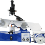
Die gleiche Schnittphysik gilt für harte, spröde Materialien, Saphir, Siliziumkarbid und kristallines Silizium verhalten sich alle unter einer Drahtsäge ähnlich. Deshalb Hart - und Sprödmaterialschneiden Wird als eine Ingenieursdisziplin behandelt, und warum Präzisions-Diamantdrahtsägeanlagen Pro Material abgestimmt sind.
Wafer-Grade und Qualitätsparameter

Nicht jede Anwendung braucht einen makellosen Wafer, und wenn Sie es nicht tun, ist die Bezahlung eines solchen ein leises Budgetleck. Wafer werden in Qualitäten verkauft, die Oberflächenqualität gegen Preis eintauschen.
| Klasse | Qualität | Am besten für |
|---|---|---|
| Prime | Gerätequalität; engste Ebenheit, geringste Mängel | Produktions-ICs und -Geräte |
| Test | Etwas geringere Oberflächenqualität; kleinere Schönheitsfehler, noch funktionstüchtig | Prozessentwicklung, FuE |
| Dummy / Monitor | Mechanischer/Prozess-Platzhalter, nicht gerätegerecht | Werkzeugabstimmung, Handhabungstests |
| Zurückfordern | Aufbereitet/gestreift und neu poliert | Kostensensitive Monitor - und Testläufe |
Ingenieure überspezifizieren häufig erstklassige Wafer für unkritische Arbeiten und zahlen Gerätepreise, um einen Prozess abzustimmen, den ein Test- oder Reclaim-Wafer gut bewältigen würde. Eine einfache Regel hilft: Wenn der Wafer zu einem versandten Gerät wird, kaufen Sie Prime; Wenn es ein Schritt auf dem Weg dorthin ist, erledigt normalerweise eine niedrigere Note die Aufgabe. Reclaim-Wafer, Prim- oder Testwafer, bei denen frühere Schichten entfernt und die Oberfläche neu poliert wurden, werden häufig als Monitorwafer wiederverwendet, gerade weil sie die Fab-Kosten unter Kontrolle halten, ohne das Produkt zu beeinträchtigen. Qualitätsmetriken, die die gleichen Qualitäten vom Spezifikationsblatt trennen: TTV, Bogen, Kette, Partikelanzahl und Widerstandstoleranz.
Silizium vs. SiC vs. GaN: Auswahl eines Wafer-Materials

Silizium dominiert nach Volumen, ist aber nicht das einzige Wafermaterial, und für manche Jobs ist es das falsche, was den Pick entscheidet, ist normalerweise die Bandlücke, die festlegt, wie viel Spannung und Wärme ein Material nehmen kann, bevor es sich nicht mehr wie ein Halbleiter verhält.
| Material | Bandlücke | Herausragende Eigenschaft | Am besten passen |
|---|---|---|---|
| Silizium (Si) | ~1,1 eV (indirekt) | Günstiger, reichlicher, ausgereifter Prozess | Logik, Speicher, die meisten Chips |
| Siliziumkarbid (SiC) | ~3.3 eV (breit) | Hohe Spannung, hohe Temperatur, hohe Wärmeleitfähigkeit | EV-Wechselrichter, Leistungselektronik |
| Galliumnitrid (GaN) | ~3,4 eV (breit) | Schnelles Schalten, hohe Frequenz | Ladegeräte, HF, Stromumwandlung |
| Galliumarsenid (GaAs) | ~1,42 eV (direkt) | Hohe Elektronenmobilität, Lichtemission | HF, Mikrowelle, LEDs/Laser |
| Indiumphosphid (InP) | ~1,34 eV (direkt) | Infrarotoptik | Faseroptisch, Photonik |
Warum Silizium immer noch die meisten Jobs gewinnt
- Niedrigste Kosten pro Fläche in der Größenordnung
- Jahrzehnte reifer Fab-Prozesse
- Natives Oxid macht die Isolierung einfach
- Stabil bis ~1.400°C im Prozess
- Wo die große Bandlücke gewinnt
- Hochspannungsleistung (SiC) über den Grenzwerten von Silizium
- Hochfrequenzschaltung (GaN)
- Besseres Wärmehandling, kleinere Anlagen
- Höhere Material- und Schneidkosten
Schnellentscheidungsregel: für allgemeine Logik und Speicher ist Silizium die Voreinstellung Für Hochspannungs-Stromumwandlung, EV-Antriebe, IndustriewechselrichterSiliziumkarbid-Waferschneidsäge Territorium gewinnt bei Effizienz und Wärme Für schnelle Ladegeräte und RF, GaN. Wenn Sie SiC speziell wiegen, unsere tiefer Leitfaden zu Siliziumkarbid als Material Bedeckt Polytypen und Eigenschaften im Detail Diese Kristalle mit großer Bandlücke sind noch härter und spröder als Silizium, weshalb sie wie das Schneiden geschnitten werden Saphir mit einer DrahtsägeAnforderungen an eine strengere Kontrolle von Draht und Vorschub.
Anwendungen von Siliziumwafern

Sobald sie die Waferherstellung durchlaufen haben, landen Siliziumwafer in fast jedem elektronischen System. Ihre Einsatzbreite ist leicht zu unterschätzen:
- ✔ Logik- und Speicher-ICsMikroprozessoren und DRAM/Flash, wo ein einzelner Chip Milliarden von Transistoren aufnehmen kann Die Mikroprozessor Ist das Festzeltbeispiel.
- ✔ StromversorgungsgeräteDioden, MOSFETs und IGBTs, die Strom in allen Bereichen verwalten, von Telefonladegeräten bis hin zu Netzwechselrichtern.
- ✔ SolarzellenPhotovoltaik-Wafer wandeln Sonnenlicht direkt in Strom um und machen einen großen Anteil der globalen Waferfläche aus.
- ✔ MEMS und SensorenBeschleunigungsmesser, Drucksensoren und Mikrofone, die direkt in Silizium geätzt wurden.
- ✔ Bildsensoren und PhotonikCMOS-Kamerasensoren und Siliziumwellenleiter für optische Daten.
Solar lohnt es sich hervorzuheben, da es die mit Abstand größte Waferflächennutzung und die kerfempfindlichste ist, weshalb Photovoltaikhersteller zuerst Diamantdraht und dünnere Wafer schoben. Geräte, die PV-Steine schneiden, wie ein spezielles Gerät Solarpanelschneidemaschine, ist so konstruiert, dass aus jedem Kilogramm Silizium mehr Wafer herausgedrückt werden.
Branchenausblick: Siliziumwafermaterial im Jahr 2026

Der Wafermarkt wächst stetig statt explosionsartig Die Schätzungen variieren je nach Umfang, aber Fortune Business Insights Beziffern Sie den Markt für Siliziumwafer im Jahr 2025 auf etwa $11,4 Milliarden und steigen Sie im Jahr 2026 auf etwa $12,1 Milliarden. BCC-Forschung Verfolgt das breitere Segment der Halbleiter-Siliziumwafer von einer $13,8 Milliarden Basis in Richtung $20,2 Milliarden, eine jährliche Rate von etwa 6,7% bis 2030. Diese Zahlen unterscheiden sich, weil die Bereiche unterschiedlich sind, aber die Richtung ist konsistent: einstelliges, nachfrageorientiertes Wachstum.
Im Jahr 2026 lohnt es sich, drei Schichten einzuplanen. Erstens, 300 mm Konsolidierung geht weiterWird von KI-Beschleunigern, Automobilelektronik und Edge Computing angetrieben, während 450 mm in der Vorproduktion weiterhin ins Stocken geraten. Zweitens, Materialien mit großer Bandlücke wachsen schneller als Silizium; Insbesondere die Nachfrage nach SiC-Wafern wächst jährlich im zweistelligen Bereich, wenn Elektrofahrzeuge und Energieanwendungen skaliert werden, obwohl Silizium das Volumenrückgrat bleibt. Drittens, Das Schneiden wird immer schlanker: Dünnere Wafer und feinerer Diamantdraht sind die Haupthebel zum Schneiden der zuvor beschriebenen Schnittfugenverluste, und dieser Trend geht eindeutig um Ertragsökonomie.
Wenn Sie Wafer oder Kapazität für ein Projekt im Jahr 2026 angeben, besteht der praktische Schritt darin, 300 mm für Siliziumvolumenarbeit anzunehmen, separat für SiC oder GaN zu budgetieren, wenn Ihr Design leistungs- oder HF-lastig ist, und die Slicing-Ausbeute als zu behandeln Linienstück und nicht als nachträglicher Einfall, denn bei den heutigen Siliziumpreisen ist Kerf echtes Geld.
Häufig gestellte Fragen
F: Warum sind Siliziumwafer so teuer?
Antwort anzeigen
Es ist nicht der Sand Kosten entstehen durch die Raffination von Silizium auf 9 11 Neuner Reinheit, das energieintensive Kristallwachstum, den langsamen Schneideschritt (wo ein großer Teil des Kristalls als Schnittfuge verloren geht), und das Läppen, Ätzen, Polieren, das nötig ist, um die Sub-Mikron-Flachheit zu treffen Enge Fehler - und Widerstandstoleranzen treiben es weiter an Das Rohmaterial ist billig; die Präzision ist das, wofür Sie bezahlen.
F: Welche Länder führen die Versorgung mit Siliziumwafern an?
Antwort anzeigen
Die Produktion von Polysilizium und Rohsilizium konzentriert sich auf China, während eine kleine Gruppe von Unternehmen in Japan (wie Shin-Etsu und SUMCO), Taiwan (GlobalWafers) und Deutschland das fertige Angebot an Prime-Wafern dominiert. Der Markt ist ungewöhnlich konzentriert: Eine Handvoll Unternehmen stellen die meisten High-End-300-mm-Wafer der Welt her, und der Lieferantenwechsel ist langsam, da jede Fab Wafer für Monate vor der Produktion gegen ihren eigenen Prozess qualifiziert. Diese Konzentration, kombiniert mit der mehrjährigen Vorlaufzeit für den Aufbau neuer Kapazitäten, ist der Grund dafür, dass die Wafer-Versorgungssicherheit in der Industriepolitik immer weiter zum Ausdruck kommt und Käufer zunehmend langfristige Mengenvereinbarungen abschließen, anstatt Spot zu kaufen.
F: Wie dick ist ein typischer Siliziumwafer?
Antwort anzeigen
Dickenwaagen mit Durchmesser, pro SEMI M1. Ein 100-mm-Wafer läuft etwa 525 µm, 200 mm etwa 725 µm und 300 mm etwa 775 µm. Spezielle verdünnte Wafer für gestapelte oder flexible Geräte können weit unter 100 µm gehen, aber diese benötigen zusätzliche Handhabungspflege, weil sie zerbrechlich sind.
F: Können Siliziumwafer zurückgewonnen oder wiederverwendet werden?
Antwort anzeigen
Ja. Gebrauchte Prim - oder Testwafer können ihre Oberflächenschichten abisolieren lassen und zu Reclaim-Wafern neu polieren, dann als Monitor - oder Dummy-Wafer für Werkzeugkalibrierung und Prozesskontrollen wiederverwendet werden, es ist eine Standardpraxis zur Kostenkontrolle in Fabs und berührt nicht die eigentlichen Produktwafer.
F: Was ist die größte Siliziumwafergröße in der Produktion?
Antwort anzeigen
300 mm (12 Zoll) ist der Volumenstandard. Ein 450-mm-Übergang ist bei den Ausrüstungskosten und der Fehlerkontrolle ins Stocken geraten, daher sind 300 mm die praktische Obergrenze im Jahr 2026.
F: Wie werden Siliziumwafer aus dem Barren geschnitten?
Antwort anzeigen
Eine Diamantdrahtsäge schneidet den gesamten Barren auf einmal mit einer Bahn aus parallelen Drahtdurchgängen, die mit Diamantkörnung beschichtet sind. Sie ersetzte das Sägen älterer Aufschlämmungen, da sie eine schmalere Schnittfuge schneidet (ca. 6080 µm gegenüber 200 µm), schneller läuft und weniger Silizium verschwendet. Nach dem Schneiden werden die Wafer kantengeschliffen, geläppt, geätzt und poliert, bis sie endgültig fertig sind.
Hartes, sprödes Kristalle schneiden?
Kerf-Verlust und die geschnittene Ebenheit entscheiden über Ihre Waferausbeute. Sehen Sie, wie speziell gebaute Diamantdrahtsägen Silizium, SiC und Saphir mit einer schmaleren Schnittfuge und einem engeren TTV schneiden.
Warum wir diesen Leitfaden geschrieben haben
Wir entwerfen und bauen Diamantdrahtsägen zum Schneiden von Silizium, Siliziumkarbid und Saphir, sodass wir den Schnittschritt aus nächster Nähe sehen, einschließlich der Schnittfugenverluste, die die meisten Waferübersichten weglassen. Die Zahlen zu Dicke, Qualität und Bandlücke stammen hier aus SEMI-Standards, veröffentlichten wissenschaftlichen Arbeiten zum Wafer-Slicing und benannten Marktforschungsquellen, wobei Marketingansprüche von Anbietern in unseren Zitaten bewusst weggelassen werden.
Referenzen und Quellen
- Wafer (Elektronik)Wikipedia
- Czochralski-prozessWikipedia
- Float-Zone-siliziumWikipedia
- Float-Zone-Silizium für die Produktion von Solarzellen mit hohem VolumenHarvard ADS (akademische Aufzeichnung)
- Fortschritte und kritische Herausforderungen beim Schneiden dünner Halbleiterwafer (MSSP, 2025)Universität Strathclyde (Strathprints)
- Grundlagen der PhotovoltaikUS-Energieministerium
- Czochralski-Silizium (PVCDROM)PVEducation (Arizona State University)
- MikroprozessorEncyclopædia Britannica
- Marktgröße und Ausblick von SiliziumwafernFortune Business Insights
- Markt für Halbleiter-SiliziumwaferBCC-Forschung
- SEMI M1, Spezifikation für polierte monokristalline Siliziumwafer (SEMI International Standards)
Verwandte Artikel
- Siliziumwafer-Schneiddraht-Säge, wie Diamantdraht Barren mit minimalem Schnittfuge schneidet
- SiC-Wafer-Schneidsäge, Schneiden von Siliziumkarbid mit großer Bandlücke
- Siliziumkarbid: Eigenschaften, Polytypen und Verwendungen
- Saphirschneiddrahtsäge, Schneiden eines der härtesten Substrate
- Solarpanel-Schneidemaschine, Maximierung der Wafer pro Kilogramm Silizium