
Neem contact op met DONGHE Company


gan wafer snijden slaagt wanneer de bewerking, de volledige substraatstapel, de machinearchitectuur en de acceptatietest samen worden gedefinieerd. Eén instelling die een vrijstaand GaN-substraat scheidt, kan een verwerkte GaN-op-siliciumwafel beschadigen, terwijl een schoon ogende in blokjes gesneden rand nog steeds elektrische, optische of stroomafwaartse montagecontroles kan uitvallen.
Bijgewerkt augustus 2026.
GaN wafelsnijden is niet één proces. Het omvat het snijden van kristallen of substraten, het singuleren van apparaat-wafers en scribe-and-cleave-bewerkingen. Kies apparatuur alleen na het identificeren van de drager, laagstapel, dikte, snijdiepte, thermische en deeltjeslimieten, en de metingen die een acceptabel resultaat definiëren.
Snelle procesopdracht
- Scheid het in bulk snijden van in blokjes gesneden bewerkte wafels voordat u gereedschappen vergelijkt.
- Behandel gepubliceerde waarden als experimentspecifiek, niet als productiestartrecepten.
- Registreer de kristaloriëntatie met energie, voeding, kracht, koeling, werkvastheid en verbruiksomstandigheden.
- Laat het proces los tegen rand-, ondergrondse, maat-, reinheids- en apparaatfunctiecriteria.
Wat houdt GaN Wafer Cutting eigenlijk in?
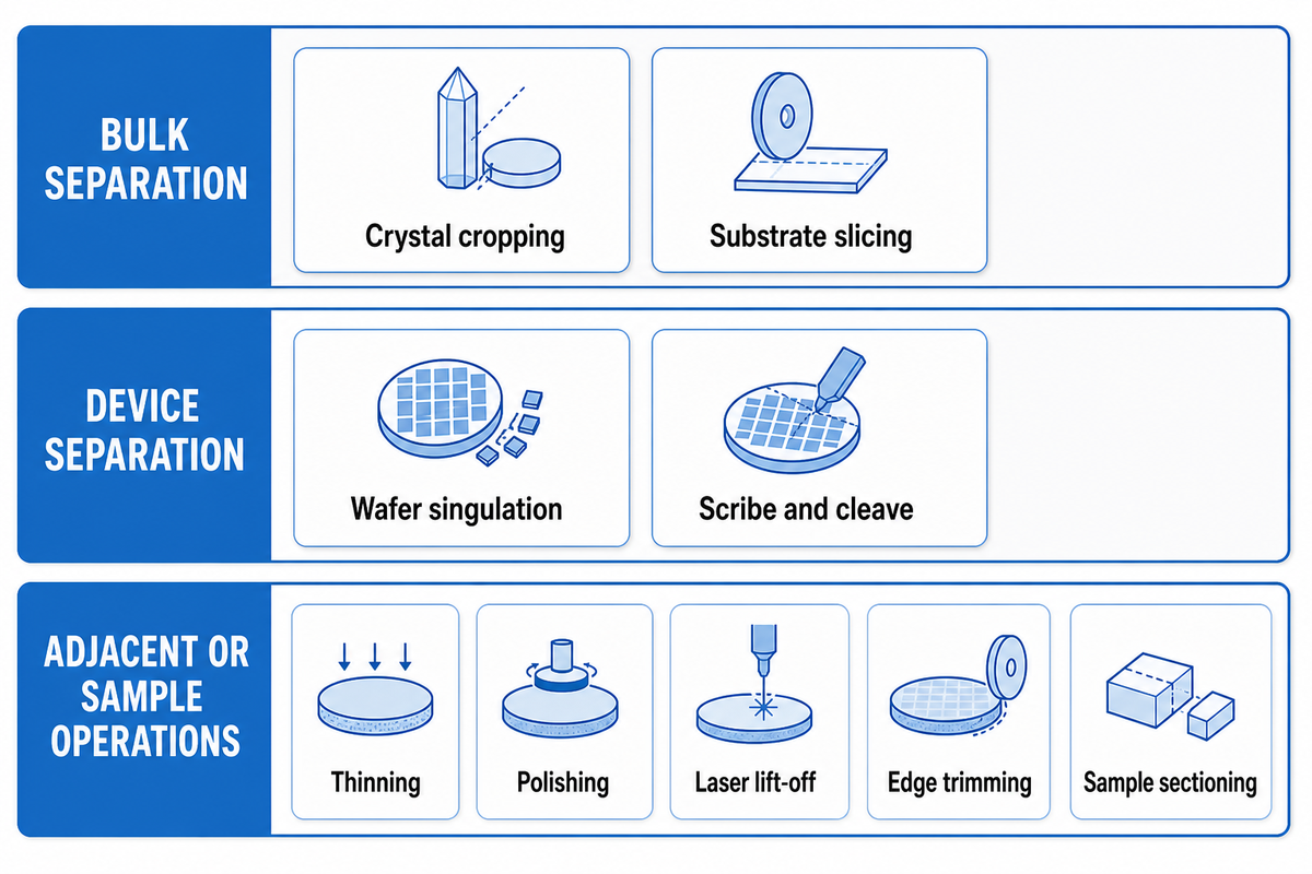
GaN-wafelsnijden kan betekenen dat een gegroeid kristal in substraten wordt gesneden, een dikke coupon wordt gescheiden, een verwerkte halfgeleiderwafel in dobbelstenen wordt gesplitst of een gecontroleerde lijn wordt beschreven voor splitsing. Verdunnen, lappen, polijsten en epitaxiale groei zijn aangrenzende bewerkingen, maar ze zijn niet uitwisselbaar met de snede zelf.
Dat onderscheid verandert het vereiste bewegings - en schademodel Bulkslicing verwijdert materiaal door de dikte van een hard en bros kristal Apparaat-wafer dicing volgt straten tussen actieve structuren, waar metallisatie, passivatie, tape, een drager, of een heterogeen substraat de thermische en deeltjesgrenzen kan instellen Kristallijn GaN mag geen splitsingsaannames overnemen van GaAs of een ander III-V materiaal Dat Wetenschappelijke rapporten GaN-snij-experiment gebruikte een vrijstaande n-type c-vlakwafel van 400 µm; de resultaten beschrijven interne lasersnijden, geen algemeen recept voor matrijsscheiding.
| Operation | Invoer | Vereiste uitvoer | Niet hetzelfde als |
|---|---|---|---|
| Kristalteelt | Boule of dikke bouillon | Referentievlak of bruikbaar segment | Wafering |
| Substraat snijden | Enkel kristal | Dun substraat met gecontroleerde kerf | Apparaatdicing |
| Wafer singulatie | Verwerkte wafer | Individuele halfgeleiderapparaten | Terugslijpen |
| Schrijf en klieven | Kristal met bruikbaar splitsingsgedrag | Gerichte breuk | Volledige diepteablatie |
| Dunner worden | Gebonden of ondersteunde wafel | Verminderde wafeldikte | Scheiding |
| Polijsten | Gesneden of grondoppervlak | Lagere ruwheid en schade | Materiaalverdeling |
| Laser-uitschakeling | Epitaxiale film op een drager | Interface scheiding | Straatdicing |
| Rand trimmen | Wafer omtrek | Gecontroleerde diameter en rand | Matrijsscheiding |
| Voorbeeldsectie | Coupon of mislukte dobbelsteen | Metrologie toegang | Productie release |
Veelgemaakte fout: een onderzoek dat zegt dat alleen “cut a GaN wafer” laat de leverancier raden of de output een substraat, een testcoupon of een functionele dobbelsteen is Vermeld de operatie in één zin en neem de inkomende en uitgaande geometrie op Voor een bredere uitleg van de mechanische route, zie draadzagen in de productie van wafels.
Waarom de Substraatstapel de Snijbeslissing verandert
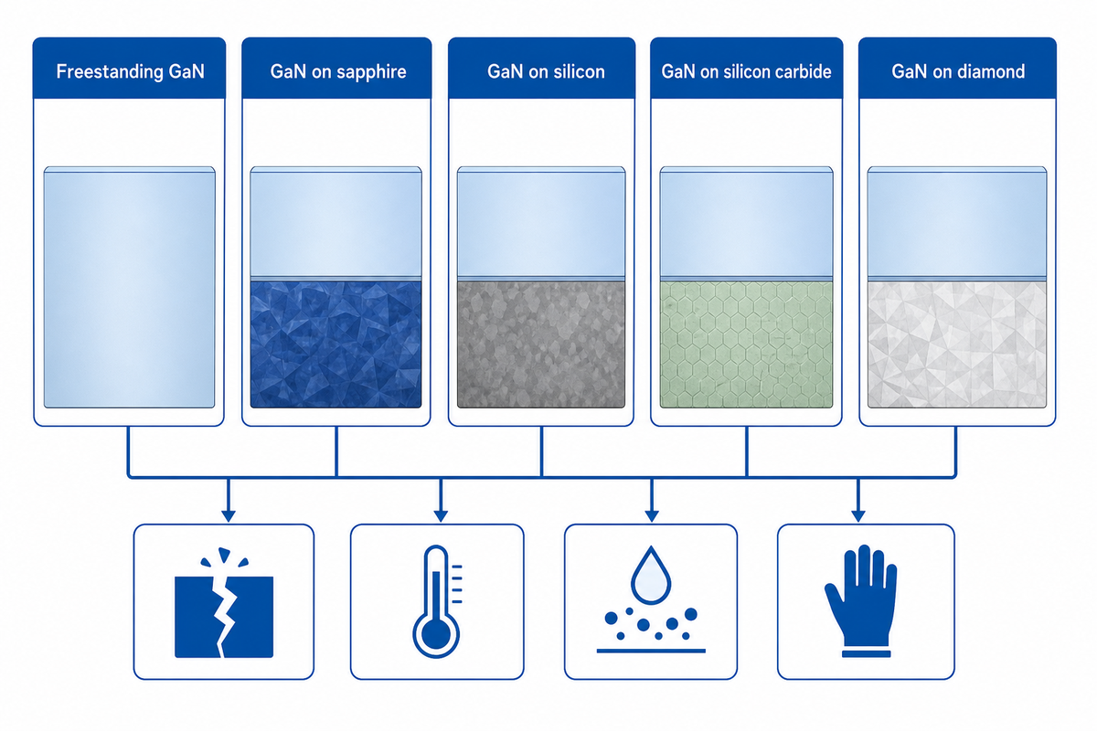
De substraatstapel bepaalt welke laag belasting draagt, waar spanning zich concentreert, hoe warmte de kerf verlaat en of puin actieve structuren kan raken Vrijstaande GaN, GaN op saffier, GaN op silicium, GaN op siliciumcarbide en GaN op diamant vereisen daarom afzonderlijke route- en kwalificatierecords. Voor deze halfgeleider met een brede bandafstand kunnen epitaxiale groei en dragerselectie de snijgrens veranderen, zelfs als de bovenste GaN-kristallaag er hetzelfde uitziet.
GaN Stack-to-Cut Compatibiliteitsenvelop
De GaN Stack-to-Cut Compatibility Envelope is een grenskaart die elke laag en interface verbindt met breuk-, thermische, verontreinigings- en behandelingslimieten.
Maak een lijst van elke laag, de dikte, de verwerkte staat, de tijdelijke binding, de metallisatie, de passivering en het blootgestelde oppervlak Voeg boeg en schering toe voordat u een snijroute kiest In één Imec GaN-op-200 mm siliciumverpakkingsprogramma, het terugslijpen van een apparaatwafel op een drager van 1.150 µm produceerde een kettingblad van 700.900 µm. Conventioneel zagen was in dat geval niet haalbaar; lasergroeven gevolgd door mechanisch zagen beperkt afbrokkelen en barsten. Deze resultaten ondersteunen een voorwaardelijke hybride route, geen algemene bewering dat hybride snijden altijd beter is.
Beschouw twee nominaal “GaN”-taken Eén geval is een vrijstaand substraat zonder patroon dat dicht bij de snede kan worden ondersteund en later kan worden gepolijst Een ander geval is een dunne GaN-laag op silicium met afgewerkte apparaten, metaal, passivatie, een tijdelijke drager en meetbare boeg. Draad- of laseromstandigheden die stabiel lijken op het eerste monster zeggen weinig over interface-delaminatie, chippen aan de achterkant, tape-laden of elektrische lekkage op de tweede. Vergelijking begint met een stapelteken- en acceptatieplan, niet met het matchen van het GaN-label. Daarom moeten procesontwikkelingsrecords naast elk resultaat de drager, dikte, oriëntatie en stroomafwaartse werking benoemen.
Key takeaway
Een overdraagbaar recept vereist een overdraagbare stapel Als de drager, interface, dikte, oriëntatie of armatuur verandert, heropen dan het procesvenster.
Apparatuuropties: draadzaag, blokjes, laser, krasblad en plasma
Geen enkele apparatuurfamilie is het beste bij alle GaN-snijbewerkingen Draadzagen passen op bulk- of dikvetsnijden; bladen bieden gevestigde straatdicing; lasers concentreren energie zonder contact met het blad; scribe-cleave maakt gebruik van kristallografische breuk; en plasma verwijdert blootliggend straatmateriaal, maar brengt controles op maskering, chemie en ionenschade met zich mee. Laserverwerking kan gebruik maken van een gepulseerde laser in de vrije ruimte of een waterstraalgeleide laserarchitectuur; deze gereedschapssystemen vereisen afzonderlijke procesparameters en bewijsmateriaal.
“Diamond wire sagen (DWS) is de primaire fase in de halfgeleiderindustrie voor het snijden van harde en brosse materialen.”
| Route | Gebruik wanneer | Primaire bedieningselementen | Bewijs nodig | Beperkingen /niet geschikt voor |
|---|---|---|---|---|
| Enkeldraadszaag | Dikke voorraad, kortingsbonnen, snijden in kleine volumes | Draadtoestand, snelheid, voeding, spanning, koelvloeistof | Kerf, ruwheid, drift, ondergrondse schade | Geen standaard voor dunne-apparaatstraten met patronen |
| Multi-draadzaag | Parallelle wafelsnijden uit geschikte kristallen voorraad | Webgeometrie, draadslijtage, krachtbalans, thermische drift | Waferdikte, totale diktevariatie, boog, opbrengst | Slechte pasvorm voor eenmalige complexe matrijspaden |
| Diamantblad | Toegankelijke straten en beheersbare mechanische belasting | Blootstelling van het mes, spil, voer, koelvloeistof, tape | Voor/achter chippen, kerf, matrijssterkte | Vermijd wanneer warpage of broze interfaces de ondersteuningsmogelijkheden overschrijden |
| Volledige diepte laser | Smalle paden of weinig mechanisch contact | Golflengte, pulsbreedte, energie, focus, snelheid, passages | Door hitte beïnvloede zone, herafzetting, tapsheid, functie | Niet acceptabel wanneer thermische of puinlimieten niet zijn geverifieerd |
| Interne laser snijden | Transparant-genoeg bulkmateriaal en gecontroleerde interne modificatie | Focusdiepte, pulsenergie, rooster, oriëntatie | Scheidingskracht, beschadigde laag, ruwheid | Gepubliceerde vrijstaande GaN-waarden zijn niet stapeloverdraagbaar |
| Laserschrijver + kleef | Kristal- en straatgeometrie ondersteunen gerichte breuk | Schrijf diepte/breedte, snelheid, energie, splijtbelasting | Scheurpad, facet, puin, apparaatuitvoer | Afwijzen wanneer de splitsing door actieve gebieden buigt |
| Lasergroef + zaag | Een beproefde stapelspecifieke groef kan mechanische scheiding begeleiden | Groefgeometrie, uitlijning, resterende diepte, bladbelasting | Zowel voor - als achterkantschade plus doorvoer | Over het algemeen niet superieur; voegt uitlijnings- en processtappen toe |
| Plasma-dicing | Masker- en straatontwerp maken op etsen gebaseerde singulatie mogelijk | Masker, chemie, bias, ionenenergie, eindpunt | Zijwand, residu, elektrische schade, doorvoer | Niet schadevrij; GaN-specifiek bewijs voor plasma-dicing is beperkt |
| Mechanisch kloof | Er bestaan een gevalideerd splitsingsvlak en zaadkenmerk | Oriëntatie, inkeping/scribe, armatuur, laadpad | Scheurafwijking, terrassen, overleving van de dood | Vermijd onregelmatige fracturen of dichte actieve lay-outs |
Een peer-reviewed AlGaN/GaN plasma-etsenstudie gekoppelde ionenenergie boven een drempelwaarde voor fysieke en elektrische degradatie. Het is geen proef met plasma-dicing, maar het is voldoende om te verwerpen. Non-contact betekent schadevrij.“ Voor mechanische snijcontext betekent DONGHE's samengestelde halfgeleider draadzaagmachines pagina is een aangrenzende SiC-applicatiereferentie, geen onafhankelijk GaN-bewijs en geen bron van overdraagbare GaN-instellingen.
Wanneer u geen draadzaag voor GaN kiest
Kies geen draadzaag alleen maar omdat GaN een hard halfgeleidermateriaal is Bewijs uit de recensie van 2024 ondersteunt draadzagen voor het snijden van wafels, terwijl de kritische beoordeling van geavanceerde die singulatie laat zien dat de kwaliteit van de verwerkte wafels ook afhangt van chippen, delaminatie, kerfgeometrie, vervuiling, schade aan de zijwand en matrijssterkte.
Dunne actieve wafels met smalle straatjes, metaal dicht bij de rand, zware boeg of nultolerantie voor drijfmest en deeltjes vereisen mogelijk een mes-, laser-, plasma-, kloof- of gekwalificeerde hybride route. Omgekeerd mag u een draadzaag niet afwijzen voor dik kristal, substraatsnijden, bijsnijden of monsterparticeren waarbij een lage contactkracht, stoepcontrole en flexibele geometrie van belang zijn. Vraag een monsterafsnijding aan op de eigenlijke stapel en vergelijk de volledige afwerkingstoeslag en inspectielast.
GaN-beslissingsboom voor snijroutes
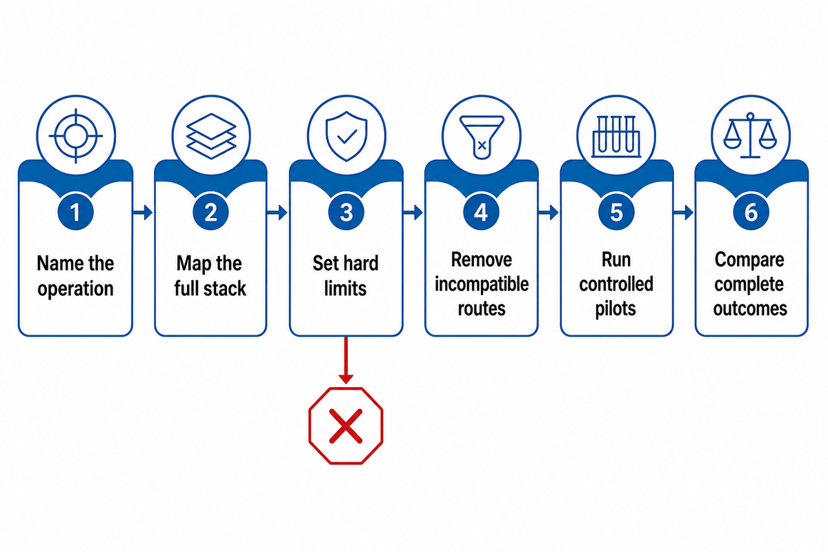
De veiligste eerste route wordt gekozen door vier vragen in volgorde te beantwoorden: Wat wordt er gescheiden? Wat draagt de lading? Welke schadekanalen zijn diskwalificerend? Welke metingen kunnen het resultaat verifiëren? Apparatuursnelheid of nominale kerf hoort na die antwoorden thuis, niet vóór hen.
GaN-beslissingsboom voor snijroutes
De GaN Cutting Route Decision Tree verwijdert incompatibele methoden voordat een piloot kwaliteit, doorvoer en downstreamkosten vergelijkt.
- Noem de operatie 1. Snijden, bijsnijden, snijden, snijden of krassen.
- Breng de volledige stapel in kaart 1. Elke drager, film, apparaatlaag, verbinding en blootliggend oppervlak.
- Stel harde limieten in 1. Kerf, temperatuur, deeltjes, randuitsluiting, scheurlengte en stroomafwaartse verwijdering.
- Incompatibele routes verwijderen elke methode waarvan de belasting, hitte, chemie of toegang een harde limiet schendt.
- Bestuurde piloten uitvoeren op zijn minst een gecentreerde toestand en begrensde veranderingen op representatief materiaal.
- Vergelijk complete uitkomsten 1. Reiniging, polijsten, inspectie, slijtage van het gereedschap en overleving van het apparaat.
Voor een bulk- of vrijstaand substraat, shortlist snijroutes en controleer of oriëntatie, kerfverlies, oppervlakteruwheid en ondergrondse schade passen bij de polijstvergoeding. Voor een wafel met patroon kunt u uitgaan van straatgeometrie, dragerondersteuning, boeg, hitte, masker, deeltjes en gevoeligheid voor actieve apparaten. Speciale taken met interne diameter of perifere snede kunnen ook herziening rechtvaardigen verticale interne snijapparatuur, maar apparatuurarchitectuur heeft nog steeds een op monsters gebaseerde match nodig.
Parametervenster met zeven signalen: wat u moet controleren en opnemen
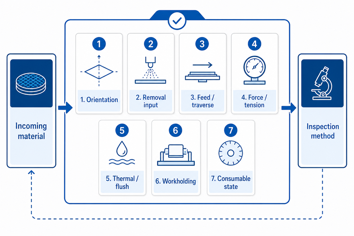
Een nuttig GaN-snijparametervenster registreert zeven gekoppelde signalen: kristaloriëntatie, verwijdering of energie-invoer, voeding of verplaatsing, kracht of spanning, thermische en spoelomstandigheden, werkvastheid en trillingen, en verbruiksomstandigheden. Het optimaliseren van één getal terwijl de andere zes driften een resultaat opleveren dat niet kan worden gereproduceerd.
Zeven-Signaal Parameter Venster: 7-Signaal GaN Controle Matrix
Het venster met zeven signalenparameters is een machine-specifiek proefrecord dat regelbare inputs verbindt met meetbare defecten en stopomstandigheden.
Deze signalen interageren Eén 2023 single-crystal GaN laserstudie vond dat vermogen, scansnelheid, scantelling en herhalingsfrequentie de groefgeometrie, door hitte beïnvloede zone en materiaalverwijdering beïnvloedden, inclusief parameterinteracties; discrepantie tussen model en experiment werd in dat onderzoek gerapporteerd onder 9,5%. Eén 2026 oriëntatiestudie meer uitgesproken faseovergang, dislocaties en diepe scheuren langs de ene onderzochte richting gevonden dan de andere Record snijrichting, zelfs als het machineprogramma ongewijzigd is.
400 µmvrijstaande wafeldikte in het onderzoek uit 2021
532 nmstudiespecifieke lasergolflengte
40 μmgerapporteerde schaal met beschadigde laag
20 cm²/sgerapporteerde, niet-geoptimaliseerde scansnelheid
| Signal | Draad/bladvoorbeelden | Laser/plasmavoorbeelden | Reactie en stopconditie |
|---|---|---|---|
| 1. Oriëntatie | Kristalvlak, snijrichting | Scanrichting ten opzichte van kristal en apparaat | Stop op richtingsscheur of facetafwijking |
| 2. Verwijderingsinvoer | Draadsnelheid, schurend, bladbelichting | Golflengte, pulsbreedte, energie, bias | Spoorkerf, groef, hitte, herafzetting |
| 3. Voer/traverse | Werkfeed en in-/uitreisprofiel | Scansnelheid en passafstand | Stop met forcepiek, onvolledige snede of scheurgroei |
| 4. Kracht/spanning | Draadspanning, spilbelasting, snijkracht | Kleefbelasting of scheidingskracht | Stop op drift, boog, draadafbuiging of onstabiele breuk |
| 5. Thermisch /spoelen | Koelvloeistofstroom, temperatuur, filtratie | Assist gas, pluimverwijdering, chuck temperatuur | Stop met temperatuurdrift, residu of herschikking |
| 6. Werkbezit | Armatuuroverspanning, tape, drager, trillingen | Chuck vlakheid, focus stabiliteit, masker ondersteuning | Stop met bewegen, focusfout of delaminatie |
| 7. Verbruiksstaat | Draadslijtage, schurende toestand, bladverband | Optica netheid, masker conditie, elektrode toestand | Stop met een tijd-trendverschuiving voorbij de controlegrenzen |
| Binnenkomend materiaal | Batch, dikte, boog, oppervlaktetoestand | Absorptie, filmstapel, straatlagen | Quarantaine ongeëvenaarde partijen |
| Inspectiemethode | Microscopie, profilometrie, cross-sectionele beoordeling | Raman, elektrisch, optisch, residuanalyse | Vergelijk geen resultaten van ongelijke methoden |
Een kwalitatieve screeningmatrix kan lage, centrale en hoge niveaus gebruiken zonder te doen alsof het universele waarden zijn Houd de oriëntatie, armatuur, koelvloeistof, verbruiksstuk en inspectieconstante vast. Varieer de voeding op drie begrensde niveaus en herhaal vervolgens de middenconditie op twee verwijderingsinputniveaus. Meet kracht of machinebelasting, stoeprand, ruwheid, versnippering, thermische signatuur en de verwijderingsvergoeding in de volgende stap. Als het midden zich herhaalt, onderzoek dan de verbruiksslijtage, trillingen, vloeistofcondities of materiaalbatch voordat u het factoreffect interpreteert. De berekening is eenvoudig: drie voedingsproeven plus twee verwijderingsinvoercontroles plus één centrale herhaling is gelijk aan zes sneden, maar de technische waarde komt voort uit gecontroleerde vergelijkbaarheid, niet het aantal runs. Gebruik de algemene draadzaag parametergids voor de machinevariabele context stelt u GaN-waarden op uw materiaal vast.
Eén gepubliceerd voorbeeld laat zien waarom scope-labels ertoe doen. Dat vrijstaande GaN-experiment uit 2021 maakte gebruik van een tweetraps sub-nanoseconde 532 nm-proces: 1,6 µJ-pulsen met een interval van 8 × 10 µm, gevolgd door 0,6 µJ op een raster van 1 µm. De auteurs rapporteerden ongeveer 40 µm beschadigde laag en 10 20 µm ruwheid aan elke gescheiden zijde, met een scansnelheid van ongeveer 20 cm²/s waarvan zij zeiden dat deze niet geoptimaliseerd was. Deze waarden documenteren één experiment; het zijn geen instellingen voor GaN-on-on-on-saffier, GaN-on-sawaterie, GaN-on-on-sawaterie-seegzaag-suiker of een productiewafel.
Best Practices van Pilot Cut tot Production Release
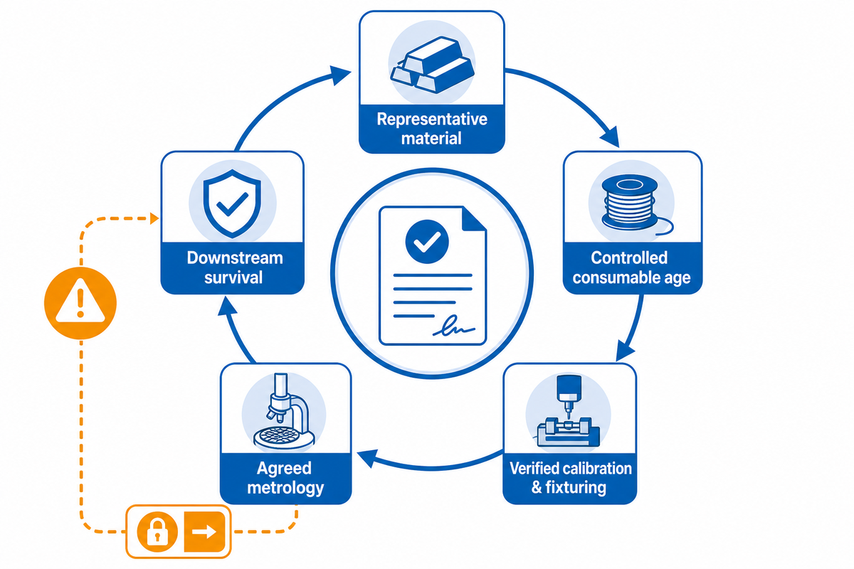
Eén succesvolle monsterafsnijding is screeningbewijs, geen productiebewijs. De vrijgave vereist herhaalbaarheid over representatief materiaal, gecontroleerde verbruiksduur, geverifieerde kalibratie en bevestiging, stabiele reiniging en hantering, overeengekomen metrologie, overleving stroomafwaarts en gedocumenteerd eigendom van procesveranderingen.
Kerf-to-Yield Verificatielus
De Kerf-to-Yield Verificatieloop verbindt inkomend materiaal, snijsignalen, edge evidence, downstream verwerking en apparaatfunctie in één release record.
Schrijf acceptatiecriteria vóór de eerste piloot Basislijn van de machine, revisie van de armatuur, kalibratiestatus, verbruiksbare partij, koelmiddel - of gasconditie en operatorvolgorde Scherm de route en voer vervolgens een begrensde matrix uit op representatieve partijen Inspecteer zowel de snede als de gevolgen: reinigingslast, polijsttoeslag, montage, draadverbinding of matrijsbevestiging, en uiteindelijk elektrisch of optisch gedrag waar actieve apparaten aanwezig zijn.
Een GaN-laserdiodelijn illustreert de kloof tussen uiterlijk en functie. Het Ferdinand-Braun-Institut-programma gebruikte 355 nm, 30 ns-pulsen bij 20 kHz voor GaN-laserstructuren in het c-vlak; de geteste secties waren 7,5 mm breed, de staven waren 1.300 µm lang en de schriftgeleerden zaten 70 µm van het p-contact. Sneller scannen verminderde uitgebreide oppervlaktescheuren, en laser-skip-and-scribe produceerde minstens twee keer zoveel goed gebroken staven als diamantrand-scribing in dat programma. Het team mat ook de lichtstroom-spanningsroutes; drempelstroomdichtheid, drempelspanning, kopieerichtingsinstellingen, het kopieerrendement, vergelijkbaar met de geometrische.
Houd het vrijgavevenster gebonden aan het goedgekeurde substraat, de waferdikte, oriëntatie, machine, armatuur, verbruiksartikel, revisie van het recept en inspectiemethode Een nieuwe batch-, drager-, film-, straatindeling, draad, mes, optische trein, masker of onderhoudsgebeurtenis zou een gedefinieerde beoordeling moeten activeren in plaats van een stille parameteraanpassing. De SEMI-normen levenscyclusbegeleiding is ook een herinnering om de huidige reikwijdte en status van elk document waarnaar wordt verwezen te verifiëren; het beoordeelde materiaal leverde geen universele GaN-snijstandaard.
Problemen oplossen met versnippering, ruwheid, drift en thermische schade
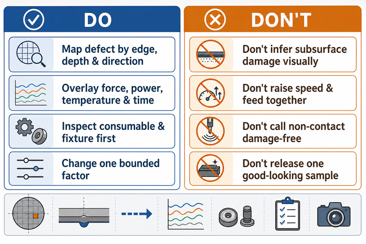
GaN-snijdefecten moeten vóór een instellingsverandering worden gediagnosticeerd op basis van locatie, oriëntatie en tijdstrend. In- en uitgangsverchopping, willekeurige randbreuk, stijgende ruwheid, geleidelijke snijafwijking, delaminatie, door hitte beïnvloed materiaal en residu wijzen op verschillende combinaties van stapel-, armatuur-, verbruiks-, machine- en vloeistof- of hulpoorzaken.
Do
- Breng elk defect in kaart op rand, diepte en kristalrichting.
- Overlaykracht, stroom, vermogen, temperatuur en tijd.
- Inspecteer het verbruiksartikel en de armatuur voordat u opnieuw afstemt.
- Verander één begrensde factor en herhaal een centrale voorwaarde.
Niet doen
- Diagnose van ondergrondse schade door het uiterlijk van het bovenoppervlak.
- Verhoog snelheid en voer samen zonder responsmatrix.
- Bel plasma of laser inherent schadevrij.
- Geef een correctie vrij op één visueel goed monster.
Chippen geconcentreerd bij het in - of uitstappen richt eerst de aandacht op ondersteuning, voerovergang, blootstelling aan verbruiksartikelen en lokale stress Ruwheid die stijgt met het aantal snijwonden suggereert slijtage, belasting, verwijdering van koelvloeistof of vuil, terwijl een onmiddellijke ruwheidssprong verandering van materiaal of opstelling suggereert Drift vraagt om gids, spanning, spil, podium, focus, armatuur en trillingscontroles Een verduisterde rand, herschikking, puinhalo, Ramanverschuiving, lekkageverandering of optisch verlies vereist thermisch onderzoek en onderzoek naar materiaalinteracties in plaats van een cosmetische reiniging.
De eerste reparatiebeweging moet bewijsmateriaal bewaren Bewaar afbeeldingen, snijrichting, batch, verbruiksleeftijd, machinetracering, vloeistofconditie, armatuurrevisie en metrologie-instellingen Een correctie zonder een vergelijkbare voor/na-registratie kan de oorzaak verbergen en de volgende excursie moeilijker te beheersen maken.
Inspectiestatistieken die beslissen of de snede acceptabel is
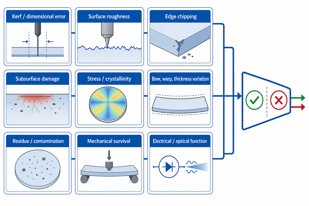
Een acceptabele snede voldoet aan de eisen van de volgende bewerking, niet alleen aan een visuele standaard. Meet geometrie, oppervlakte- en randschade, ondergrondse of thermische effecten, wafelvorm waar van toepassing, netheid, mechanische overleving en representatieve elektrische of optische prestaties voor actieve apparaten.
| Metrisch | Method | Bemonsteringslocatie | Acceptatie eigenaar |
|---|---|---|---|
| Kerf /dimensionale fout | Optische metrologie of gekalibreerde beeldvorming | Ingang, midden, uitgang; meerdere assen | Ontwerp en proces |
| Oppervlakteruwheid | Profilometrie of microscopie | Over het snijvlak en de oriëntatie | Polijsten /proces |
| Rand chippen | Optische of scanning-elektronenmicroscopie | Voor, achter, hoeken, straat | Quality |
| Ondergrondse schade | Cross-sectionele microscopie of gekwalificeerde proxy | Slechtste snijzones | Materialen /proces |
| Stress/kristalliniteit | Raman of diffractiemethode | Rand-naar-interieur lijnscan | Materials engineering |
| Boog, schering, diktevariatie | Geometrie metrologie | Volledige wafer kaart | Waferproces |
| Residu /verontreiniging | Visuele, chemische of deeltjesanalyse | Straat, actieve rand, achterkant | Contaminatiecontrole |
| Mechanische overleving | Behandeling, montage of sterktetest | Representatieve matrijs/substraten | Montage / betrouwbaarheid |
| Elektrische/optische functie | Apparaatspecifieke test | Rand-nabij en besturingsapparaten | Apparaattechniek |
A GaN-on-sapphire laserdicing-onderzoek gerapporteerde Raman-piekverschuivingen binnen ongeveer 40 µm van de chipranden en brachten deze in verband met lokale spanningsrelaxatie. Die waarneming verschilt van de ongeveer 40 µm beschadigde laag gerapporteerd in het vrijstaande interne snijonderzoek van GaN. Soortgelijke cijfers betekenen niet hetzelfde mechanisme of dezelfde meting. Definieer de methode, bemonsteringslocatie en acceptatie-eigenaar naast elke limiet.
Wat verandert er in GaN Wafer Processing in 2026?
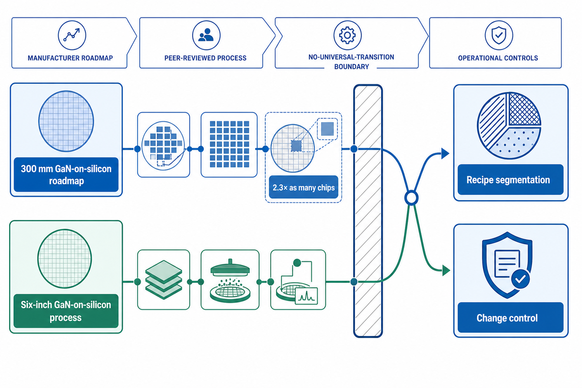
GaN-procesplanning in 2026 moet tegelijkertijd meer waferschalen en meer heterogene stromen accommoderen De praktische implicatie is strengere receptsegmentatie, automatisering, metrologie en veranderingscontrole, niet een universele stap naar één diameter of één snijmechanisme.
Infineon kondigde in 2025 een 300 mm GaN-op-silicium-routekaart aan en geplande eerste klantstalen voor het vierde kwartaal van 2025, met 2,3 keer zoveel chips per 300 mm wafer als op 200 mm Dat is een toegeschreven fabrikant roadmap Een aparte 2026 peer-reviewed 15 cm GaN-op-silicium apparaatproces gebruikte een siliciumsubstraat van 675 µm, vermaalde het tot 400 µm en vormde een membraan van 600 µm met behulp van diep reactief ionenetsen. Samen vertonen de bronnen gelijktijdige schaal- en integratiepaden in plaats van een uniforme overgang.
Als u apparatuur in 2026 specificeert, vraag dan hoe recepten, armaturen, waferkaarten, verbruiksgeschiedenis en inspectielimieten zijn gerangschikt op stapel en diameter. Vereisen dat de leverancier de omschakeling en traceerbaarheid op representatief materiaal aantoont. Behandel generieke groeivoorspellingen van verbindingen en halfgeleiders alleen als achtergrond; ze bewijzen niet de vraag naar een bepaalde GaN-snijroute.
RFQ en Sample-Cut Checklist
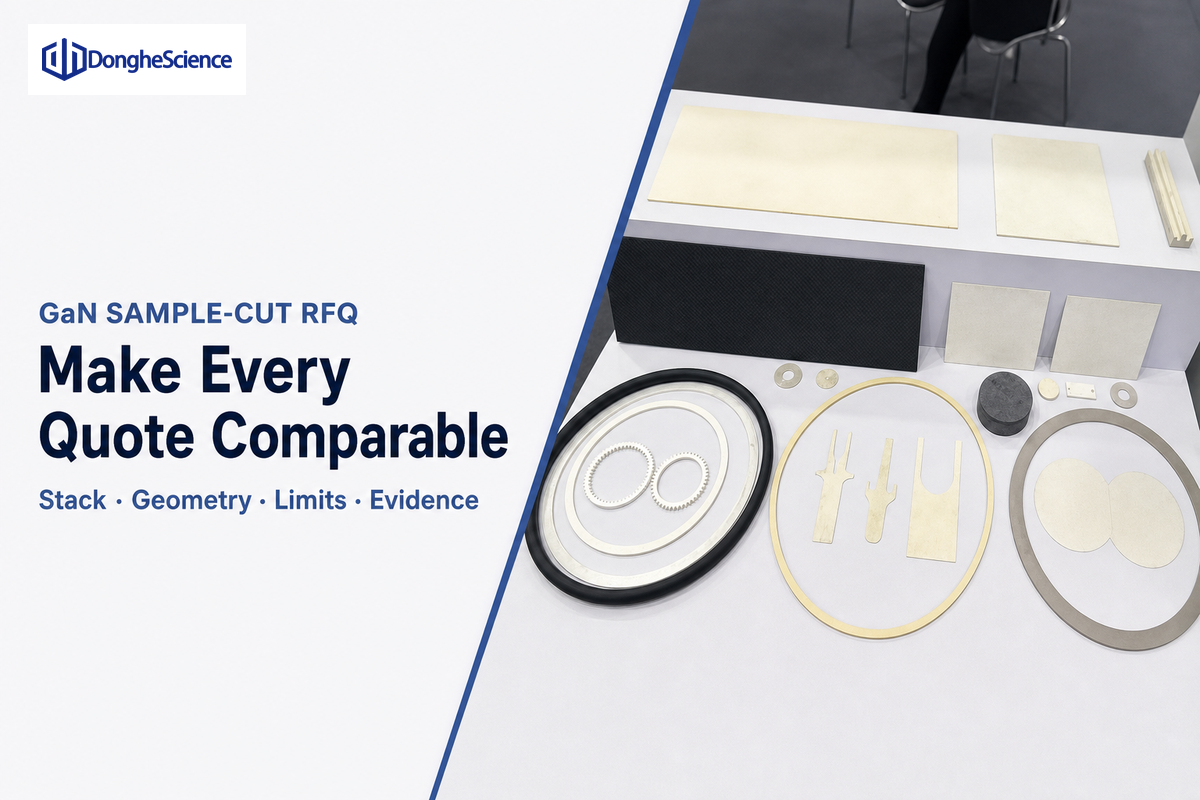
Een vergelijkbare GaN-snijofferte heeft een gecontroleerd invoerpakket, een gedefinieerd resultaat en bewijsvereisten nodig. Stuur dezelfde stapeltrekking, geometrie, kwaliteitsdoelen, monstertelling en downstream-beperkingen naar elke leverancier; anders beschrijven prijs- en cyclustijdreacties niet dezelfde taak.
RFQ checklist kopieer deze naar uw offerteaanvraag
| Parameter | Vereiste invoer | Waarom het ertoe doet | Bewijs terug |
|---|---|---|---|
| Materiaal en stapel | Elke laag, drager, binding, film | Stelt breuk-, hitte- en verontreinigingslimieten in | Route grondgedachte |
| Geometrie | Diameter, dikte, tekening, pad | Definieert reizen, diepte en ondersteuning | Armatuur- en vermogensverklaring |
| Verwerkte toestand | Ongepatroont, epi, metaal, passivatie, apparaten | Verandert aanvaardbare deeltjes en warmte | Handling en reinigingsplan |
| Kristaloriëntatie | Vliegtuig, uitsnijding, snijrichting | Verandert breuk en materiaalverwijdering | Uitlijningsrecord |
| Kwaliteitslimieten | Kerf, chip, ruwheid, schade, vorm | Voorkomt alleen visuele acceptatie | Gemeten rapport |
| Verontreiniging / thermische limieten | Toegestane vloeistoffen, ionen, deeltjes, temperatuur | Beschermt actieve oppervlakken en interfaces | Verklaring inzake compatibiliteit van processen |
| Doorvoerbasis | Lotgrootte, uptime, inspectie en reiniging | Maakt cyclustijd vergelijkbaar | Getimede procesuitsplitsing |
| Voorbeeldplan | Hoeveelheid, partijen, controles, retentie | Tests herhaalbaarheid en batch-effecten | Geserialiseerde resultatenset |
| Veranderingscontrole | Goedgekeurde machine, verbruiksartikel, armatuur, recept | Behoudt kwalificatie | Herzienings - en kennisgevingsvoorwaarden |
Vraag naar ruwe metingen en monsteridentificatoren, niet alleen geselecteerde foto's Een serieuze beoordeling moet uitsluitingen zichtbaar maken: niet-ondersteunde prestatieprojecties, parameters geleend van silicium of SiC, en claims die slechts op één goed monster zijn gebaseerd Voor een bredere toepassing van de toepassing, vergelijk precisie diamant draadzaag toepassingen en dan een GaN-specifiek testplan aanvragen.
Veelgestelde vragen
Is GaN beter dan silicium voor stroomapparaten?
Het hangt af van het apparaat en het systeemdoel.
Galliumnitride kan hoogfrequente en hoogvermogen-dichtheid transistorontwerpen in vermogenselektronica ondersteunen, terwijl silicium in veel toepassingen kosten, productierijpheid en leveringsvoordelen behoudt Spanning, schakelfrequentie, thermisch pad, pakket, betrouwbaarheid, besturingsontwerp en totale systeemkosten moeten het materiaal bepalen Vergelijk een specifiek GaN-apparaat met een specifiek siliciumapparaat onder dezelfde bedrijfstaak in plaats van een universele rangschikking toe te passen.
Wat is het GaN wafelsnijproces?
Het proces begint met het benoemen van de scheidingsoperatie.
Een GaN-snijproces brengt de substraat- en apparaatstapel in kaart, selecteert een compatibele snij- of singulatieroute, ontwikkelt een gekoppeld parametervenster en inspecteert rand-, ondergrondse, dimensionale en verontreinigingseffecten. Vervolgens bevestigt het de compatibiliteit van reiniging, polijsten, assemblage en apparaat voordat de vrijgegeven machine, armatuur, verbruiksartikel, recept en metrologie worden vergrendeld. Bulkslicing en bewerkte wafer-dicing vereisen verschillende faalmodellen en bewijsmateriaal.
Hoeveel kost GaN wafersnijden?
Een verdedigbare kostprijs heeft de volledige route nodig.
Kosten zijn afhankelijk van materiaalwaarde, werking, stapel, monster - of partijgrootte, machinetijd, levensduur van verbruiksartikelen, kerfverlies, reiniging, inspectie, polijstvergoeding, schrootrisico, en kwalificatiewerkzaamheden Vergelijk kosten per geaccepteerd substraat of matrijs na downstreamverwerking, niet alleen machinecyclustijd Een prijsklasse zonder die inputs is niet beslissingswaardig.
Waar kan ik galliumnitridewafels kopen?
Geef de wafer op voordat u een leverancier selecteert.
Vraag diameter, dikte, oriëntatie en off-cut, vrijstaande of epitaxiale stapel, drager, doping of geleidbaarheid, oppervlakteafwerking, boeg en schering, defectlimieten, randprofiel, traceerbaarheid en inspectiegegevens. Kwalificeer de wafel tegen het beoogde snij- en stroomafwaartse proces in plaats van alleen op de materiaalnaam te kopen.
Kan een diamantdraadzaag GaN-substraten snijden?
Ja, voor geschikte snij- en snijbewerkingen.
A peer-reviewed overzicht uit 2024 omvat GaN onder hard brosse halfgeleidermaterialen die zijn verwerkt door diamantdraadzagen. De geschiktheid hangt nog steeds af van de vraag of het werk bestaat uit bulk snijden, bijsnijden of monstersnijden; de kristaloriëntatie en geometrie; toegestane kerf- en ondergrondse schade; stijfheid van de machine; grenswaarden voor koelvloeistof en vervuiling; en polijsten na het snijden. Er mag niet worden aangenomen dat het blad-, laser-, plasma- of kloofmethoden voor wafels van verwerkte apparaten vervangt. Vraag de leverancier om de machinearchitectuur, draad, armatuur, koelvloeistof, monitoringsignalen en inspectiemethoden te identificeren en valideer vervolgens het exacte materiaal en acceptatieplan met geserialiseerde monsterstukken van representatieve partijen.
Is galliumnitride giftig?
Gebruik de huidige veiligheidsgegevens voor het daadwerkelijke materiaal en proces, inclusief stof, slurry, koelvloeistof, gas, plasmabijproducten, opnieuw afgezet materiaal en reinigingsafvalstromen.
Hanteringscontroles niet alleen uit de afgewerkte vaste stof Beoordeel de veiligheidsgegevens van de leverancier, de lokale blootstellings- en afvalregels en het stof, de slurry, het koelmiddel, het gas, de plasmabijproducten of het opnieuw afgezette materiaal dat ontstaat door snijden en reinigen. Gebruik gekwalificeerde industriële hygiëne- en milieuprocedures voor de faciliteit en het proces.
Bereid een GaN-monster-cut-verzoek van beslissingskwaliteit voor
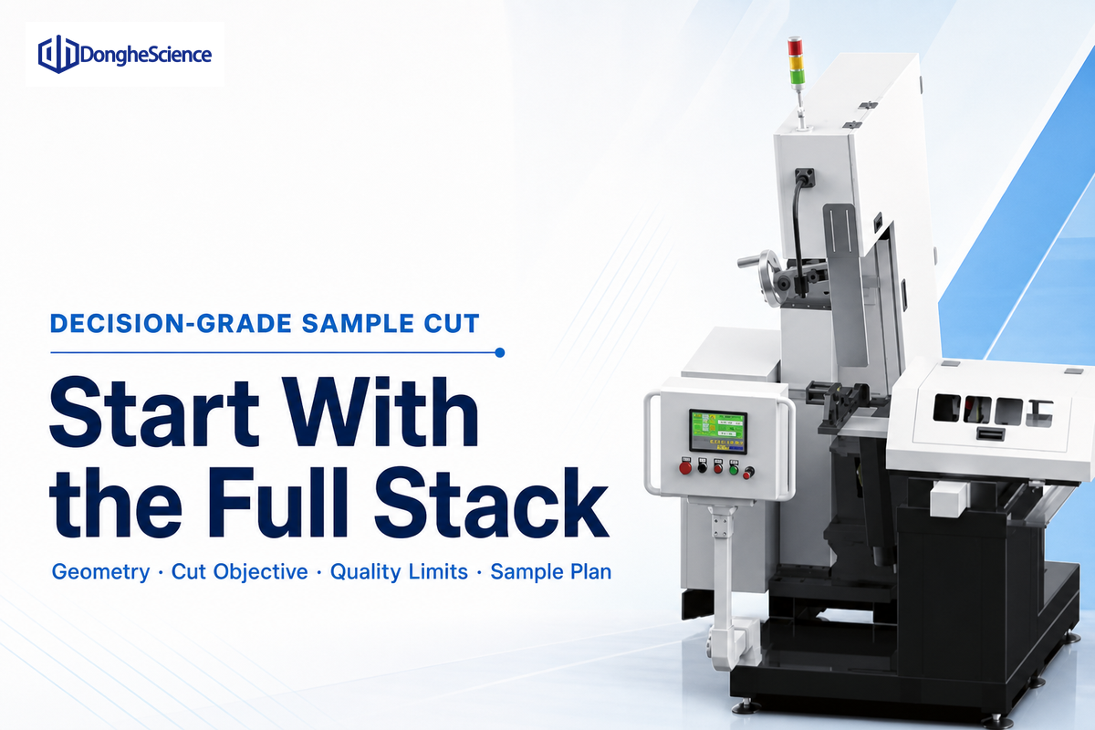
DONGHE ontwerpt diamantdraadzaagapparatuur voor de verwerking van hard en bros materiaal Deel de volledige stapel, geometrie, snijdoelstelling, kwaliteitslimieten en monsterplan, zodat de eerste discussie de draadzaagpassing kan scheiden van methoden die een andere route nodig hebben.
Referenties en bronnen
- Hogesnelheidslasersnijden van galliumnitride Wetenschappelijke rapporten
- Diamant draad zagen review Tijdschrift voor productieprocessen
- Die singulatietechnologieën voor geavanceerde verpakkingen Tijdschrift voor Vacuümwetenschap en Technologie B
- GaN laserverwerkingsparameterstudie Materiaalkunde in halfgeleiderverwerking
- Oriëntatie-afhankelijke GaN laserschade studie International Journal of Mechanical Sciences
- GaN laserdiodeschrijven en functionele metingen Ferdinand-Braun-Institut
- Raman-studie nabij met laser in blokjes gesneden GaN-op-saffierranden Materiaalkunde in halfgeleiderverwerking
- Plasma-geïnduceerde schade in AlGaN/GaN-structuren Micro-elektronische techniek
- Fabricagestroom van GaN-op-silicium-apparaten van 15 cm Microsystemen en nanotechniek
- Normen veelgestelde vragen SEMI

![Polysiliciummateriaal: eigenschappen, kwaliteiten en gebruik [Gids]](https://wiresawcutter.com/wp-content/uploads/2026/08/polysilicon-material-featured-768x512.webp "Polysiliciummateriaal: eigenschappen, kwaliteiten en toepassingen in de zonne- en halfgeleiderindustrie 13")


![Polysiliciummateriaal: eigenschappen, kwaliteiten en gebruik [Gids]](https://wiresawcutter.com/wp-content/uploads/2026/08/polysilicon-material-featured-150x150.webp)