Get in touch with DONGHE Company
-
Phone: +86 181-1645-5490
-
Email: Sales18@DongheScience.com

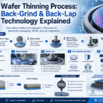
Diamond Wire Saw for Photovoltaic
High-Precision Diamond Wire Saw for Photovoltaic
Advanced diamond wire saw for photovoltaic technology delivering precision silicon wafer cutting with 75% faster throughput and 22% reduced kerf loss for solar cell manufacturing.
75%
Faster Speed
22%
Material Savings
50%
Less Damage

What Is A Photovoltaic Diamond Wire Saw?
The diamond wire saw for photovoltaic is a precision cutting tool specifically designed to slice silicon ingots into ultra-thin wafers employed for solar cell production. This advanced technology becomes industry standard in wafer cutting for photovoltaic applications.
Core Definition
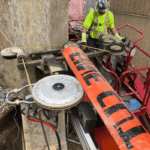
Diamond wire saw technologies need a high-strength steel core wire generally with an industrial-coated diamond particle typically of 36-80μm diameter to make precision cutting into monocrystalline and polycrystalline silicon for photovoltaic applications.
Core Components
Understanding the type and design of diamond wire used for slicing photovoltaic wafers is essential for making the right selection.
Steel Core Wire
Top tenacity steel wire from 36μm to 80μm ranges in diameter. A core with thinner cross section reduces kerf width but demands that a precise control be maintained in tension during cutting.
Diamond Particles
Industrial diamond play the role of cutting by abrasive action, where its particle size ranges from 8 to 25μm. It is directly associated with the pad for the finishing effect on the surface.
Bonding Layer
Diamonds are electroplated and then bonded to the core using a chemical bonding process with resin matrix. The bonding strength determines the wire life in the cutting of solar silicon wafers.
Solar Wafer Slicing Equipment: Manufacturing Supply Chain Position
Step 01
The Production Of Polysilicon
Raw polysilicon is material of choice for applications in photovoltaic generation for solar energy.
Step 02
Ingot Formation
Monocrystalline or polycrystalline ingots are formed that are used to fabricate solar wafers.
Step 03 / Focus
Diamond Wire Sawing
The silicon ingot is cut into very thin wafers around some 150-180 μm thick using photovoltaic diamond wire saw technology.
Step 04
Solar Cell Processing
Then wafers are processed to develop functional photovoltaic cells with electrical contacts.
Step 05
Module Assembly
The cells are grouped to form solar panels for their usage.
Market Overview: Diamond Wire Saw For Photovoltaic Industry
The global market for diamond wire saw systems as used in the photovoltaic production sector has seen extraordinary growth, courtesy the expansion of solar power right across the globe:
$3.2B
Market Size By 2024
11.5%
CAGR 2024-2033
$8.5B
Projected 2033
120M+
Meters Wire/Year
How the Diamond Wire Saw For Photovoltaic Works
The diamond wire saw cutting method in photovoltaic silicon consists of different steps which are perfectly coordinated mechanically:
01
Wire Web Setup
A number of diamond wires are arranged in parallel to form a web for cutting multiple wafers at the same time
02
High-Speed Motion
The wire operates at a speed of 10-20 m/s and moves back and forth
03
Workpiece Feed
Silicon ingot is introduced into the wire web at a rate that is controlled
04
Coolant Flow
A coolant that is water-based helps to get rid of the debris and keep the temperature in check
In the course of solar wafer cutting, the diamond grains that are attached on the wire surface function as cutting edges and take away the silicon through a process that combines ductile and brittle fracture. The secret of getting high-quality photovoltaic wafers is through keeping the cutting conditions optimal which favor ductile-mode cutting; this, in turn, results in smoother surfaces with very little percentage of subsurface damage.
Why Diamond Wire Saw for Photovoltaic vital for the Solar Industry
The use of diamond wire saw technology by the photovoltaic industry is an indication of the remarkable advantages over traditional slurry-based cutting methods. For solar cell producers, these benefits literally imply improvements in their bottom lines.
Technology Comparison
| Parameter | Diamond Wire | Slurry Wire | Advantage |
|---|---|---|---|
| Cutting Speed | 10-20 m/s | 4-8 m/s | 75% faster |
| Kerf Loss | Low | High | Savings |
| Coolant | Water-based | PEG slurry | Eco-friendly |
| Surface (Ra) | 0.3-0.5μm | 0.5-0.8μm | Superior |
| Min Thickness | 120μm | 160μm | Thinner |
Economic Impact
30%+
Silicon Savings
2-3×
Throughput
40%
Less Post-Process Cost
60%
Less Equipment
“Nowadays, with better wire speeds, only 16 slicers are needed per GW compared to 40 in 2016.”
Environmental Sustainability
Water-based coolants replace toxic PEG oil-based slurries
Kerf recycling allows extraction of high-purity silicon
Narrow kerf means less material entering waste streams
Lower energy consumption per wafer due to speed
Smaller facility footprint requires fewer resources
💎 Free Online Tool
Diamond Wire Saw Machine Price Cost Calculator
Real-time cost estimation per wafer. Modify any parameter to see immediate results.
Production Parameters
$0.000
Cost Per Wafer
0
Wafers/Ingot
0h
Cycle Time
$0
Monthly Cost
📊 Cost Breakdown
📉 Wire Diameter Comparison
✓
Recommended Cutting Parameters
Wire Speed
18 m/s
Range: 15-22 m/s
Feed Rate
0.6 mm/min
Range: 0.4-0.9 mm/min
Wire Tension
32 N
Range: 28-38 N
Kerf Loss
75 μm
Expected value
⚖️ Wire Diameter Options Comparison
| Wire Ø | Kerf Loss | Wafers/Ingot | Cost/Wafer | Material Saved |
|---|
Diamond Wire Saw Types for Photovoltaic Production
Right diamond wire selection is very important to get the most out of your photovoltaic manufacturing process.
Electroplated Diamond Wire
The predominant diamond wire type for photovoltaic applications. Single-layer diamond particles are coated on the steel core. Monocrystalline silicon wafer cutting is done with high speed and uniform performance.
Best for: High-volume mono-Si production
Resin Bond Diamond Wire
Diamond particles are in layers in the resin and the wire has a long life and is self-sharpening. The wire is cutting hard materials and in PV the applications are needing wire usage for a long time.
Best for: Cost-sensitive operations
Sintered Diamond Wire
Very strong wire made from metal matrix with diamond particles being sintered. Longest wire life provided but cutting speeds are low. Resistance to extreme wear is among the reasons why it’s used in certain applications.
Best for: Thick cuts, hard materials
Ultra-Fine Wire (36μm)
Most advanced thin-core wire technology that gives the least kerf loss. Up to 22% materials saved when compared with traditional wire diameters. Important for cost-competitive solar cell production.
Best for: Maximum yield optimization
| Wire Type | Core Diameter | Cutting Speed | Wire Life | Kerf Width | Best Application |
|---|---|---|---|---|---|
| Electroplated | 38-45μm | High | Medium | ~70μm | Mono-Si PV Wafers |
| Ultra-Fine Electroplated | 36μm | Medium-High | Medium | ~60μm | High-Yield Production |
| Resin Bond | 40-50μm | Medium | Long | ~80μm | Multi-Si, Cost Focus |
| Sintered | 50-60μm | Lower | Very Long | ~100μm | Specialty Applications |
Diamond Wire Saw for Photovoltaic vs. Traditional Slurry Sawing
The cutting of silicon wafers has changed significantly in the photovoltaic (PV) industry due to the switch from slurry sawing with loose abrasive (LAWS) to the diamond wire saw.
| Parameter | Diamond Wire Saw | Slurry Wire Saw | Advantage |
|---|---|---|---|
| Cutting Speed | 10-30 m/s wire speed | 5-15 m/s wire speed | 75% faster |
| Kerf Loss | 60-80μm | 100-150μm | 22% less waste |
| Subsurface Damage | 5-15μm depth | 15-30μm depth | 50% reduction |
| Environmental Impact | Water-based coolant | SiC slurry + PEG | Eco-friendly |
| Silicon Recyclability | High purity kerf | Contaminated kerf | Recyclable |
| TTV | – | – | – |
| Operating Cost | Wire cost higher | Slurry cost continuous | Comparable TCO |
Reason for PV Industry Changeover to Diamond Wire Saw Technology
Photovoltaic diamond wire saw won over solar cell factories almost completely owing to its remarkable advantages.
Cost Competitiveness
22% material savings and 75% faster throughput make production economically superior even though the wire cost is higher.
Quality Improvement
Lowering the effect of subsurface damage by half results in an increase in cell efficiency and yield.
Environmental Compliance
Toxic slurry disposal difficulties are completely removed with water-based coolants.
Thin Wafer Capability
Sub-180μm wafers for next-generation solar cells can easily be produced.
Silicon Recycling
The new kerf allows high-quality silicon recovery that supports sustainability goals.
PV Wafer Slicing ROI & Yield Calculator
Estimate your efficiency gains and cost savings by optimizing for Diamond Wire Saw technology. Compare against traditional methods or optimize your current parameters.
Process Parameters
Target Wafer Thickness
150
μm
Kerf Loss (Wire Diameter + Abrasive)
50
μm
* Standard Slurry Saw: ~120μm | Diamond Wire: ~40-60μm
Silicon Ingot Length
mm
Production Economics
Annual Production Target
Million Wafers
Average Wafer Value
$
Yield Analysis
Pitch (Thickness + Kerf)
200 μm
Wafers per Ingot
2,500
Efficiency Gain vs. Slurry (120μm Kerf)
Extra Wafers / Year
+35.0 M
Potential Revenue Gain
$14.0 M
Key Benefits of Diamond Wire Saw for Photovoltaic Manufacturings
Explore the reasons why the top-ranking solar producers around the world prefer diamond wire saw technology for the manufacturing of silicon wafers.
Increased Throughput & Productivity
The cutting speed of the photovoltaic diamond wire saw is 75% faster than that of slurry methods, so throughputs are increased to the maximum production capacity of the whole plant without any additional equipment investment.
Silicon Material Waste Minimization
The advanced kerf loss reduction technology saves the glittering matter up to 22%, directly catering the cost-per-watt economics in solar cell production.
Wafer Surface Quality at its Best
The subsurface damage is reduced by 50%, which means that the surfaces of the wafers are smoother, and etching requirements are lower, thus leading to higher solar cell conversion efficiency.
TTV Control of Super Precision
The use of advanced TTV control systems results in thickness variations of less than 10μm, which means that cell performance is made consistent and yield rates in PV manufacturing are increased.
Sustainability in the Environment
The water-based coolants not only take the place of the toxic slurries but also make the recycling possible through the clean silicon kerf. 35% of the adopters regard sustainability as the main factor for the selection of diamond wire saw for photovoltaic.
Lower Total Cost of Ownership
The sum of the advantages of quicker processing, saving on material, and easier waste handling make for a very attractive TCO even though the cost of the wire is higher.
Troubleshooting Diamond Wire Saw Issues in Photovoltaic Manufacturing
Challenges can crop up in diamond wire sawing operations even if the processes are optimized. Knowing about the common issues and their respective solutions will help you to quickly fix them and thus, less production will be disrupted.
Preventing Wire Breakage in PV Wafer Cutting
Wire breakage is the number one issue at the photovoltaic diamond wire sawing arena, which can halt production and, at the same time, cause damage to ingots that are only partially-cut:
⚠️ Common Wire Breakage Causes
- Too much tension: Tension that exceeds the wire strength limits
- Accumulating wear: Loss of diamond causing the wire diameter to get below the minimum
- Pollution: Particles in the coolant creating localized stress
- Machine shaking: Resonance leading to cyclic stress fatigue
- Guide wheel damage: Worn-out grooves creating pinch points
- Ingot flaws: Presence of hard inclusions or cracks in silicon
✓ Prevention Strategies
- Tension monitoring: Real-time detection with automatic adjustment
- Scheduled wire change: Replace wire before it gets critically worn out
- Coolant filtering: Continuous filtering to 10μm or smaller
- Vibration checking: Constant monitoring and damping optimization
- Preventive maintenance: Regular inspection and replacement of guide wheels
- Ingot checking: Quality verification before cutting
Solving Surface Quality Problems in Photovoltaic Wafers
| Problem | Likely Cause | Solution |
|---|---|---|
| High surface roughness | Feed rate too high, wire speed too low | Reduce vf/vc ratio, use finer grit wire |
| Visible saw marks | Wire vibration, tension fluctuation | Stabilize tension, check guide wheels |
| Deep scratches | Loose diamond particles, contamination | Filter coolant, inspect wire quality |
| Uneven surface | Inconsistent diamond distribution on wire | Use higher quality wire, verify supplier QC |
Addressing TTV Issues in Solar Wafer Production
Total Thickness Variation (TTV) can be termed as a major parameter of quality for photovoltaic wafers, which usually demand TTV lower than 20μm as the maximum limit:
Wire web alignment
Position wires parallel across the cutting zone
Tension uniformity
Equal tension across all wires in the web
Feed system precision
Smooth, consistent workpiece movement should be checked
Thermal stability
The coolant temperature should be maintained constant in order to avoid thermal distortion
Equipment calibration
The machine geometry and alignment should be regularly checked
Selecting the Proper Diamond Wire Saw for Your Photovoltaic Production
The technology used for diamond wire saws in photovoltaic production has totally changed the process of making solar wafers, leading to a taking up of the market with the use of efficiency, accuracy, and eco-friendliness as the main selling points. The industry has over 98% adoption of this technology for monocrystalline silicon and the continuous development of super-fine wire further assures that the technology will keep playing an essential role in solar cell manufacturing for a long time.
Here are the main points that will help you to see the best in your photovoltaic diamond wire sawing operations:
1
Match the wire specifications with your needs
Take into account the target wafer thickness, the desired surface quality, and the production volume.
2
Optimize the parameters of the process systematically
The vf/vc ratio, the tension control, and the coolant management should be the focus of your efforts.
3
Adopt maintenance that is proactive
Put in place a system that will ensure you will not incur any expensive shut down costs through keeping a watch on the machines and replacing parts as per the schedule.
4
Evaluate suppliers with a broad perspective
Think in terms of the total cost of ownership and not only the wire price.
5
Be ready for the changes in technology
Get yourselves ready for wire that is thinner, wafers that are bigger, and higher sustainability standards.
Future Trends of Diamond Wire Saw in Photovoltaic Industry
The diamond wire technology for photovoltaic applications is still very dynamic. Manufacturers who have knowledge of these new trends will be able to develop the capabilities required for the future.
Market Outlook 2023-2032
$2.5B
Electroplated Market 2032
7.9%
CAGR
10%+
Diamond Wire Growth
APAC
Leading Region
Current Condition
Manufacturing of 50-60μm wire at the major companies is already in large-scale production.
Near-term Goal
45-50μm is likely to be the standard size wire by 2026-2027.
R&D Front
Laboratory is working on Sub-40μm wire for next-generation efficiency.
Main Difficulties
For thinner wires, it is difficult to cut sharply and also the life of the wires is shortened.
Equipment Needed
To control tension more accurate, and to implement improved vibration damping systems.
Diamond Wire Saw For Photovoltaic: Global Success Stories
Real-world implementation case studies demonstrating efficiency and ROI
Case Study 01: China
22% Kerf Loss Reduction for Major Chinese Manufacturer
The Challenge
The client, a top 5 solar wafer manufacturer in China, was experiencing considerable material loss with a staggering 180μm kerf width using slurry-based equipment. Silicon waste was out of control amidst rising polysilicon costs.
Our Solution
- Equipment Upgrade: Replaced 48 slurry machines with DWS-6800 series (42μm wire).
- Optimization: Tuned wire speed (18-22 m/s) and tension (22-28N).
- Eco System: Installed water-based fluid system with recycling.
| Metric | Before | After |
|---|---|---|
| Kerf Loss | 180 μm | 140 μm (-22%) |
| Speed | 0.3 mm/min | 1.1 mm/min |
| SSD | 15 μm | 7 μm |
| Savings | — | $18.5M USD |
“The ROI exceeded our projections—we recovered the full equipment investment in just 14 months.”
Case Study 02: Japan
Achieving <5μm TTV in 160μm HJT Production
The Challenge
Pioneering ultra-thin 160μm wafers for HJT cells, this Japanese manufacturer struggled with TTV control (avg 12-15μm), leading to 8% rejection rates and frequent wire breakages.
Our Solution (DWS-8000 Pro)
- TTV Control Tech: Real-time tension monitoring with ±0.5N accuracy.
- Vibration Damping: Reduced lateral vibration by 75%.
- Smart Wire Mgmt: 99.7% reliable breakage tracking.
| Metric | Before | After |
|---|---|---|
| Avg TTV | 12-15 μm | 4.2 μm |
| Rejection | 8% | 1.2% |
| Breakage | 1/800 cuts | 1/4500 cuts |
“We can now produce 160μm wafers with TTV consistently under 5μm. Achieving 26.5% cell efficiency.”
Case Study 03: Europe
Improving mc-Si Cutting for European Client
The Issue
Multi-crystalline silicon (mc-Si) presents unique challenges due to grain boundaries and inclusions, causing unpredictable cutting behavior, surface irregularities, and excessive wire wear.
Our Answer
- Adaptive Algorithm: Auto-adjusts parameters at grain boundaries.
- Custom Wire: Optimized density (280-320 grits/mm).
- Polish: Custom alkaline texturing polish (Ra 0.3-0.5um).
| Metric | Before | After |
|---|---|---|
| Defect Rate | 6.2% | 1.8% |
| Wire Usage | 2.8 m/w | 1.9 m/w |
| Uniformity | 78% | 94% |
“The adaptive cutting technology truly understands material variations. Dramatic improvements in yield.”
Case Study 04: India
Stopping Wire Breakage in High-Volume Production
The Challenge
Scaling to 10GW capacity, this Indian startup faced 12 wire breakages per machine/month, causing 200+ hours of downtime and safety risks.
SmartWire™ Solution
- 100Hz Monitoring: Detects tension micro-variations.
- Weibull Analysis: Models breakage force.
- Auto Alerts: Warns 15-20 cuts before failure.
| Metric | Before | After |
|---|---|---|
| Breakages | 12/mo | 0.8/mo |
| Downtime | 200+ hrs | 18 hrs |
| OEE | 71% | 89% |
“We went from reactive firefighting to proactive maintenance. Zero surprise breakages in six months.”
Case Study 05: USA
ROI Realization for North American Manufacturer
The Challenge
Transitioning from slurry to diamond wire required proving ROI ($28M investment) against higher US labor costs and Asian imports.
Our Approach
- Deep TCO Analysis: Included all labor, waste, and consumable costs.
- Phased Deployment: Validated 6 machines at a time.
- Consumables: Minimized per-wafer cost specs.
| Category | Slurry | DWS-7200 |
|---|---|---|
| Consumables | $8.2M | $6.1M |
| Si Savings | — | $4.8M |
| Net Benefit | — | $14.4M |
“We are now cost-competitive to imports and qualify for IRA incentives. The best capital decision we made.”
Diamond wire saw for photovoltaic FAQs
Expert insights into the mechanism, benefits, and optimization of silicon wafering.
What is a photovoltaic wafering diamond wire saw, and how does it work?
A photovoltaic wafer wire saw is basically a wire cutting machine employing a wire with bonded diamond particles for slicing silicon ingots into thin silicon wafers. The cutting wire speeds against the workpiece while the cutting fluid/slurry cools and lubricates the slice and carries away all debris. This allows cut waste that is smaller than a traditional blade-based cut. Therefore, this wire saw cutting method is widely employed in solar wafer production for monocrystalline and polycrystalline photovoltaic silicon.
Why is the diamond wire cutting method much preferred over the traditional saw blade cutting technique during solar silicon wafer manufacturing?
Industrial diamond wire sawing for slicing silicon gives precise cutting with comparatively small material loss from the reduced saw silicon kerf, better wafer quality compared to fixed diamond wire blades, and slurry sawing. This method has provided essential benefits, ensuring the slicing of thinner wafers for more surface morphology on the silicon and higher wafers’ yields for solar cells manufactured within the crystal-shop and photovoltaic cell industries, as it is recognized as an industry-leading technology in this area of the photovoltaic industry and within the global solar photovoltaic supply chain.
How does wire sawing affect the wafer quality and the performance of the photovoltaic cells?
Several cutting forces, cutting velocity, and distribution of diamond particles along the wire affect wafer quality from the wire sawing cutting processes. Adequate control of these process parameters reduces subsurface damage, improves flatness and thickness uniformity, and minimizes microcracks in the silicon wafer. Higher-quality wafers directly enhance solar cell efficiency in solar cell-industry production and favor desirable photovoltaic technology outcomes.
What kind of diamond cutting wires are used for slicing silicon ingots and ingot wafering?
Common types are an electroplated diamond wire, a fixed diamond wire, and a precision diamond wire with diamond particles or diamond cutting beads embedded in it. The choice is made depending upon the cutting capacity of the diamond wire required and the wafering thickness. Should the wire require cutting continuous monocrystalline silicon or polysilicon rods, each cutting wire will affect the cutting speed, cutting surface finish, and overall cutting method efficiency.
Do diamond wire saws have the ability to cut materials like sapphire wafers or semiconductor materials?
Diamond wire cutting and diamond wire slicing are extended to cutting hard materials beyond photovoltaic silicon, such as sapphire wafers and assorted semiconductor crystals. These include the cutting tool and process parameters such as wire speed, cutting liquid picked, and diamond grit, which are adjusted to the morphology of silicon, sapphire, and other alloy and ceramic substrates while maintaining very precise cutting and minimizing subsurface damage in wafer processing.
What are the main wire saw cutting process parameters to be optimized in PV manufacturing?
Cutting speed, wire tension, feed rate (cutting depth), diamond grit size on the wire feed, and cutting fluid flow-the key parameters for wire saw cutting, among various other less important ones-are the automation and control of these factors. These reduce the forces involved in cutting, enhance cut quality, and accelerate the rate at which substrates are sliced. Optimization translates into highly efficient cuts with uniform wafer thickness, minimal kerf loss, and higher yield in solar wafer fabrication and photovoltaic applications.
Compared to the slurry-based and blade-based cutting methods, how does the diamond-wire slicing method perform in cutting silicon ingots?
Diamond wire slicing techniques generate lesser kerf losses and good wafer flatness in comparison to the blade-based cutting method, and virtually eliminate the use of abrasive slurry in the traditional wire saw process, thus enabling cleaner cutting processes. By contrast, modern diamond wire cutting is cleaner than slurry methods, more inherently automated, and delivers a cleaner cut surface, making it the method of choice for high-volume solar cell manufacturing and wafer production.
What are the maintenance and safety considerations for a wire saw cutting machine in the photovoltaic industry?
Regular inspections of the diamond wire and cutting force process monitoring are very crucial, and such monitoring should be undertaken, as well as the timely replacement of damaged wires and proper management of cutting fluid and slurry. Safety measures taken should involve guarding moving parts, noise and vibration, and the control of particulate waste. Regular calibration and automation is a measure of maintaining the cutting capabilities of your equipment and enhancing the life of the sawing machine, and is in line with ensuring high-quality wafering of silicon for solar cell and semiconductor applications. It is straightforward in principle: regular calibration and automation are relatively low-cost measures to carry through in these ways.