Get in touch with DONGHE Company
-
Phone: +86 181-1645-5490
-
Email: Sales18@DongheScience.com

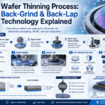
Advanced Technology
High Tech & Precision Wire Saw
The cutting-edge diamond wire saw methods designed for semiconductor, photovoltaic, and precise material processing sectors. Our top-notch cutting technology makes it possible to obtain sub-micron accuracy.
≤0.04mm
TTV Precision
60μm
Min. Kerf Width
3000m/min
Wire Speed
48%
Market Focused
Product Lineup
High-Tech Precision Cutting Solutions
Specialized diamond wire saw systems designed for the most demanding semiconductor and photovoltaic applications
Semiconductor
Bestseller
Silicon Wafer Cutting Wire Saw
High-precision multi-wire saw system for silicon wafer slicing. Achieves ultra-thin wafers with exceptional TTV control for semiconductor and electronics manufacturing.
Wafer: 2-12 inch
TTV: ≤5μm
Multi-wire
View Details
Solar Energy
High Volume
Diamond Wire Saw for Photovoltaic
Optimized for solar cell production with high throughput and low kerf loss. Reduces silicon waste while maintaining consistent wafer quality for PV manufacturing.
High yield
Low kerf
Auto-loading
View Details
Photovoltaic
Solar Panel Cutting Machine
Precision cutting system for solar panel and cell processing. Features automated handling and optimized cutting parameters for photovoltaic module production.
Panel sizes
Clean edge
High speed
View Details
Compound Semiconductor
Advanced
SiC Wafer Cutting Saw
Specialized wire saw for silicon carbide wafer processing. Handles the extreme hardness of SiC with optimized diamond wire and cutting parameters for EV and power electronics.
SiC specialist
4H/6H-SiC
EV market
View Details
Optical & LED
Sapphire Cutting Wire Saw
Precision cutting solution for sapphire substrates used in LED and optical applications. Achieves smooth surface finish and minimal sub-surface damage on hard sapphire material.
LED substrate
Low SSD
Optical grade
View Details
Ingot Processing
Ingot Cropping Wire Saw
Efficient wire saw system for silicon and compound semiconductor ingot cropping. Removes seed and tail ends with precision squaring capability for downstream processing.
Large ingots
Squaring
End cropping
View Details
Main Benefits
What Makes Our High-Tech Wire Saws Superior
High-tech engineering along with precise manufacturing results in extraordinary cutting performance
01
Super-High Precision
Sub-micron TTV accuracy provided by advanced motion control and real-time compensation systems
02
Very Low Material Loss
Ultra-thin diamond wire (0.04-0.12mm) minimizes kerf loss and maximizes yield per ingot
03
Very High Throughput
Multi-wire configurations allow for the simultaneous processing of several wafers, thus providing maximum productivity
04
Intelligent Automation
Ready for Industry 4.0 with automated wire management, loading and process monitoring
Technical Data
Performance Specifications
Detailed technical specifications across our high-tech precision wire saw lineup
| Specification | Silicon Wafer | SiC Wafer | Sapphire | Ingot Cropping |
|---|---|---|---|---|
| Workpiece Size | 2-12 inch wafers | 2-8 inch wafers | 2-6 inch substrates | Up to φ620mm ingots |
| Wire Diameter | 0.04-0.12mm | 0.06-0.15mm | 0.08-0.18mm | 0.15-0.35mm |
| TTV Precision | ≤5μm | ≤10μm | ≤8μm | ≤50μm |
| Surface Roughness | Ra ≤0.3μm | Ra ≤0.5μm | Ra ≤0.4μm | Ra ≤1.0μm |
| Wire Speed | Up to 3000m/min | Up to 1500m/min | Up to 1800m/min | Up to 2000m/min |
| Kerf Width | 60-150μm | 80-180μm | 100-200μm | 180-400μm |
| Automation Level | Full auto | Semi/Full auto | Semi auto | Full auto |
Industries
Target Applications
Our high-tech precision wire saws serve critical manufacturing processes across advanced industries
Semiconductor Manufacturing
Silicon wafer production for IC chips, memory devices, and integrated circuits powering electronics worldwide.
Solar / Photovoltaic
Silicon ingot slicing and solar cell cutting for renewable energy production and photovoltaic module manufacturing.
Power Electronics (SiC)
Silicon carbide wafer processing for EV inverters, power supplies, and high-efficiency power conversion systems.
LED & Lighting
Sapphire substrate cutting for LED chips, providing the foundation for energy-efficient lighting solutions.
Optics & Photonics
Precision cutting of optical materials for lenses, windows, and advanced photonic components.
Research & Development
Laboratory sample preparation for universities and research institutions advancing materials science.