Get in touch with DONGHE Company
-
Phone: +86 181-1645-5490
-
Email: Sales18@DongheScience.com

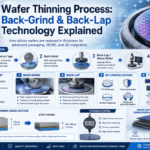
Silicon Wafer Cutting Wire Saw
Silicon Wafer Cutting Wire Saw: The Complete Guide to Diamond Wire Technology
Learn the technology for slicing precision silicon wafers and how diamond wire saw cutting machines have changed photovoltaic and semiconductor wafer production by providing increased efficiency, decreased kerf loss, and improved surface quality.
90%+
Global Wafers Use Diamond Wire
30%
Material Waste Reduction
75%
Faster Than Slurry Sawing
<55μm
Achievable Kerf Width

What is Silicon Wafer Cutting Wire Saw Technology?
Wire Saw Technology is a highly accurate machining method that changed the way solar cells and semiconductors are manufactured. Wire saw technology allows manufacturers to produce ultra-thin (20µm thick) silicon wafers that are of the highest quality while minimizing the material loss.
Definition and Core Concepts of Wire Saw for Silicon Wafer
A silicon wafer cutting wire saw is a specialized tool used to slice a silicon ingot into individual wafers. Instead of cutting with a traditional blade, silicon wafer cutting wire saw technology relies on cutting with a very thin wire that has diamond particles embedded onto it to produce very accurate slices with little kerf width and outstanding surface finish.
A core concept of wire sawing is that the diamond wire or wires continually loop around and around, or move back and forth in parallel lines, coated with industrial-quality diamond particles. These wires are then pressed against the silicon material and operate at very high speeds (10 to 25m/s). The abrasive cutting process removes the silicon material through the process of micro-grinding and therefore results in a very smooth surface and a lower rate of subsurface damage.
💡 Key Insight:
The use of silicon wafer cutting wire saws has reduced kerf width from 200-250µm (using slurry wire) down to 60-80µm (using ultra-fine diamond wire), saving up to 30% of the cost of silicon raw materials.
Evolution of Silicon Wafer Cutting: From Slurry to Diamond Wire
The silicon wafer slicing industry has changed dramatically in the last decade. Prior to the mid-2010s, the predominant technique for wafer slicing was to use slurry wire sawing, which is accomplished with steel wire and abrasive slurry. The introduction of diamond wire saw technology for silicon wafer slicing represents a turning point in manufacturing.
Today, diamond wire sawing has become the preferred process for manufacturing solar wafers and is beginning to be widely used in the semiconductor wafer dicing industry. By using diamond wire saws rather than slurry-based processes, the process of cutting is faster, the result is cleaner, and the environmental impact is significantly lower than that of slurry-based processes.
Key Components of Silicon Wafer Wire Saw Systems
Understanding the main components of a silicon wafer cutting wire saw system is essential for proper operation and maintenance:
Diamond Wire (Electroplated/Resin Bonded)
Wire Guide Rollers
Wire Tension Control System
Coolant Delivery System
Workpiece Mounting Table
Motion Control Electronics
Wire Speed Regulators
Real-time Monitoring Sensors
How Silicon Wafer Cutting Wire Saw Works
The important elements of diamond wire saw technology include determining and adapting the working principles to optimise cut performance while achieving the best surface finish during the production of silicon wafers.
Diamond Wire Cutting Mechanism for Silicon Wafers
Silicon wafers are cut using diamond wire saws which function based on fixed-abrasive machining. The cutting edge consists of diamond particles that are bonded onto a wire core either through electroplating or resin bonding, which create a series of abrasive edges, which remove silicon material via a controlled process of abrasion.
The diamond wire saw operates by moving at a rapid pace while the silicon ingot is slowly advanced into the cutting area. Cutting debris (silicon swarf) is continuously removed from the cutting area by a coolant system and the cutting temperature is maintained at optimal levels. This results in a very precise TTV (total thickness variation) control and a minimal amount of surface roughness.
Critical Process Parameters in Silicon Wafer Wire Sawing
| Parameter | Typical Range | Impact on Quality | Optimization Notes |
|---|---|---|---|
| Wire Speed | 10-25 m/s | Surface finish, cutting efficiency | Higher speeds improve throughput but increase wire wear |
| Wire Diameter | 60-120 μm | Kerf loss, wire breakage risk | Thinner wires reduce material loss but require careful tension control |
| Feed Rate | 0.3-1.0 mm/min | Production rate, surface damage | Balance between throughput and wafer quality |
| Wire Tension | 20-40 N | Cut straightness, TTV | Consistent tension critical for thin wafer cutting |
| TTV (Total Thickness Variation) | < 10 μm | Device performance, yield | Achieved through precision wire guidance |
| Surface Roughness (Ra) | 0.3-0.6 μm | Post-processing requirements | Optimized with proper coolant and wire selection |
| Wafer Thickness | 100-180 μm | Material usage, handling | Ultra-thin cutting (<100μm) requires specialized setup |
| Kerf Loss | 60-120 μm | Material efficiency | Diamond wire achieves 30-40% reduction vs slurry |
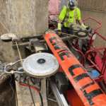
Single Wire vs Multi-Wire Saw for Silicon Wafer Slicing
Multi-Wire Saw
The multi-wire saw machine is the backbone of the highest capacity manufacturers of both solar and semiconductor wafer cutting machinery, as it is capable of producing many silicon wafers at the same time with much greater efficiency. This type of machine utilizes several hundred individual diamond wires that are arranged in a specific pattern and attached to a traditional grooved roller.
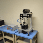
Single Wire Saw
In comparison, single wire saws are typically used to manufacture low volume and/or custom silicon wafers, provide high precision and flexibility, and enable the cutting of materials that are very difficult to machine (such as SiC and GaN). The use of single wire saws also allows manufacturers to create a variety of specialty wafer sizes and orientations based on customer request.
Types of Silicon Wafer Cutting Wire Saw Systems
All silicon wafer wire saw configurations meet specific manufacturing needs. Knowing the advantages and disadvantages of each can assist in identifying which will be best suited to meet a user’s requirements.

⚡ Electroplated Diamond Wire Saw
These saws use diamond particles bonded to a wire using electroplated nickel. They produce a more aggressive cutting force and higher material removal rates than resin bonded diamond wire saws. These saws are mainly used for the production of large volumes of solar wafers where throughput is the highest priority. Electroplated diamond wire saws are also the most commonly used style of multi-wire saws.

🔬 Resin Bonded Diamond Wire Saw
Resin bonded diamond wire saws use a resin matrix to bond the diamond particles, resulting in a smoother cutting action and a higher-quality surface finish compared to electroplated saws. They are the preferred method of cutting semiconductor wafers and precision applications requiring minimal subsurface damage. Even though they cost more than electroplated saws, they will produce a superior finish.

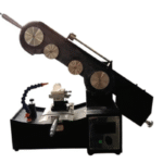
🔄 Endless Loop Diamond Wire Saw
The endless loop diamond wire saw is designed to be operated with a single-wire loop for laboratory (research), prototype and specialist material cutting, such as sapphire wafers, SiC, and GaN. As a single-wire loop system, it has the highest level of flexibility and precision available.

📊 Multi-wire Saw System
Industrial multi-wire saw systems typically use 500-2000 parallel (or more) wires to cut multiple wafer slices at the same time. Multi-wire saws dominate the PV manufacturing industry because they allow entire ingots to be cut in one operation and have the highest throughput of any mass production methods.

🎯 Precision Single Wire Saw
Precision single wire saws are designed for extreme accuracy when cutting individual samples or small batches of the same material. They are also used in SiC wafer cutting and advanced materials research. Precision saws have programmable cutting patterns and provide exceptional dimensional control.

🤖 AI Enhanced Wire Saw
These next-generation systems use machine learning algorithms to optimise the adjustability of all wire tension, cutting speed and coolant flow in real-time, based on sensor feedback, ensuring a consistent quality.
Silicon Wafer Slicing Engineer Suite
Interactive tools for Yield, Cost Analysis & Process Optimization
Wafer Yield & Kerf Loss Calculator
Total Wafers:
0
Material Efficiency:
0%
Diamond Wire vs. Slurry Cost Analyzer
Slurry Total Cost:
$0
Diamond Wire Total Cost:
$0
Potential Annual Savings:
$0
Recommended Cutting Parameters
Recommended Wire Speed
–
Typical Tension
–
Coolant Type
–
* Based on standard industry values [2025 Report]. Always consult your specific machine manual.
Industry Applications of Silicon Wafer Cutting Wire Saw
Silicon Wafer Wire Saw Technology Is Used in Many Industries, such as Solar Energy and Advanced Semiconductors. Each Industry Has Different Slicing Precision Requirements and Surface Quality Requirements.
Solar PV Manufacturing
High-volume cutting of solar wafers for mono and multi-crystalline silicon solar cells. 160-180μm standard thickness.
Semiconductor IC Fabrication
Ultra-precise cutting of silicon wafer for IC devices with surface requirements at nanometer level.
Power Electronics (SiC/GaN)
Cutting of SiC wafers and GaN wafers for the manufacture of Electric Vehicle inverters, 5G Infrastructure, and High-Power Devices.
Sapphire/LED Substrates
Precision cutting of sapphire wafers for LED manufacturing and optical devices requiring a crack-free edge.
Research Laboratories
Flexible means of cutting experimental materials, by offering custom sizes of materials to fit specific projects and working prototypes.
Battery Technology
Precise cutting of silicon anode materials and other specialty materials for next-generation energy storage systems.
RF/Microwave Devices
High-frequency wafer processing for RF/microwave device applications, which require extraordinary thickness uniformity and surface quality.
Thermal Management
Cutting of silicon and ceramic substrates for the manufacture of thermal interface materials and heat sinks.
Common Challenges in Silicon Wafer Cutting Wire Saw Operations
Silicon Wafer cutting has its inherent technical challenges, even with advanced diamond wire technology. Understanding these issues and how to resolve them can be an essential step toward optimizing wafer slicing.
High Kerf Loss in Silicon Wafer Cutting
The traditional cutting method for silicon wafers produces approximately 30 to 40 per cent of the expensive silicon cut into waste (sawing waste), thereby placing an extreme financial strain on costs.
✓ Solution: Use ultra-fine diamond wire (<50µm) to reduce kerf loss to 60-80µm.
Ultra-Thin Wafer Breakage
Wafers thinner than 100 microns are more likely to break during the wafer slicing operation because of mechanical forces and movement.
✓ Solution: Tension Control of wire and a Proper Set of Cutting Parameters.
Diamond Wire Breakage
Significant wire breakage interrupts production and increases costs. Large-volume manufacturers consider this a top concern.
✓ Solution: Actual tension measurement and AI-Powered Machine Learning Maintenance.
SiC & Hard Material Cutting
SiC hardness is nearly equal to diamond; cutting is difficult due to tool wear and edge chipping.
✓ Solution: Specialized diamond wire with optimized grit size and concentration.
Poor Surface Quality & Saw Marks
Saw marks leave deep impressions requiring extensive post-processing, increasing costs and affecting device performance.
✓ Solution: Use optimized resin-bonded wire force, coolant flow, and cutting speed.
TTV (Total Thickness Variation)
Controlling TTV variations is challenging with large-diameter Wafers because large TTVs significantly impact yield.
✓ Solution: High-accuracy wire guidance systems with closed-loop feedback control.
High Coolant Consumption
Conventional pre-cooling methods generate excessive coolant, increasing operating costs and complicating waste disposal.
✓ Solution: Advanced internal coolant recycle systems and optimized nozzle delivery.
Equipment Selection Difficulty
Selection of appropriate equipment should be based on a thorough evaluation of application requirements and manufacturer specifications.
✓ Solution: Work with experts to evaluate applications for the best-fitting solution.
Comparing Silicon Wafer Cutting Wire Saw with Other Technologies
The Industry currently uses silicon wafer cutting with wire saws as the primary method; therefore, comparisons with other technologies help determine the appropriate equipment to purchase and optimizing processes.
Diamond Wire Saw vs Slurry Wire Saw for Silicon Wafer
The most significant advancement in the history of silicon wafer slicing was the transition from Slurry-Wire-Saw technology to Diamond Wire Saw Technology:
| Parameter | Diamond Wire Saw | Slurry Wire Saw |
|---|---|---|
| Cutting Speed | 2-3x faster | Baseline |
| Kerf Loss | 200-250μm | ~200μm (comparable) |
| Environmental Impact | Water-based coolant | Oil-based slurry disposal |
| Wire Cost | Higher per meter | Lower per meter |
| Surface Quality | Generally superior | Good for some materials |
| Industry Adoption | 95%+ in solar | Legacy applications |
Wire Saw vs Laser Cutting for Silicon Wafer Processing
Wire saw and laser cutting technologies have very different applications in processing silicon wafers. Laser systems have advantages in certain applications; however, the majority of bulk wafer slicing is completed using diamond wire saws:
Wire Saw Advantages
The wire saw has a smaller heat-affected zone than other processes, making it more effective for thick ingots and enabling higher throughput for specific formats.
Laser Advantages
Laser cutting provides more precise cuts for intricate designs with no kerf loss in specific applications; it is faster on fragile materials.
Hybrid Approaches
Recent advances in technology integrate the use of both lasers to create a prescribed shape and wire saws to produce fragile wafers.
When to Choose a Wire Saw Over Other Silicon Wafer Cutting Methods
Silicon wafer cutting wire saw technology is typically the best choice when:
Processing silicon ingots for solar wafer or semiconductor wafer production
High-volume production requiring consistent quality across thousands of wafers
Standard rectangular or square wafer formats are required
Minimizing kerf loss and surface damage is important
Cutting hard materials like SiC wafer or sapphire wafer substrates
Future of Silicon Wafer Cutting Wire Saw Technology
The silicon wafer wire saw industry is evolving quickly due to the growing need for thinner wafers, more efficient manufacturing, and environmentally friendly production; understanding these trends will ultimately be valuable when creating long-term strategies and selecting appropriate machinery and methods.
AI and Machine Learning in Silicon Wafer Wire Sawing
Artificial Intelligence (AI) is changing the way that Silicon Wafer Wire Saw is done:
Predictive maintenance
Maintenance based on predictive machine learning algorithms enables the detection of component failures in advance of production interruptions.
Process optimization
AI models optimise process settings in real time to maximise yield and quality.
Real-time monitoring
Wire saws contain intelligent systems capable of real-time monitoring of quality deviations and automatically taking corrective measures.
Wire life prediction
Predictive modelling will determine when the wire should be replaced, reducing waste and ensuring consistent cut quality.
Ultra-Fine Diamond Wire Trends for Silicon Wafer Cutting
The push toward finer diamond wire continues, with industry leaders now working with wires below 35μm diameter. This trend promises significant kerf loss reduction but requires advances in wire manufacturing, tension control, and process stability.
100μm
Traditional Wire
60μm
Current Standard
<35μm
Emerging Technology
25μm
Research Target
Hybrid Cutting Technologies for Next-Gen Silicon Wafers
Hybrid techniques are emerging for producing ultra-thin wafers. For example, new methods of this type would involve cutting an original wafer with a laser beam and separating it along that line with wires, or cutting the wafers with plasma and exploiting the stress reduction inherent in the process of creating these components.
Sustainable Practices in Silicon Wafer Wire Saw Manufacturing
Environmental considerations are increasingly crucial in silicon wafer manufacturing:
Kerf loss recycling
Recovery and reprocessing of silicon debris
Coolant recovery
Closed-loop systems minimize water consumption
Energy efficiency
Improved drive systems reducing power consumption
Wire recycling
Programs for diamond and steel wire recovery
Frequently Asked Questions (FAQs)
Expert insights on Silicon Wafer cutting and Wire Saw technology.
What is the effect of the semiconductor wire sawing process on the quality of cuts made on silicon wafers?
Factors such as the speed and feed rate of the wire, the temperature at which it is sawed, the medium with which it is cut, and the type of wire saw have a significant effect on the quality of cuts being made. Optimizing the parameters for the manufacturing of monocrystalline silicon has enabled the minimization of subsurface damage and warpage in wafers, as well as improved the wafer surface finish, including both roughness and flatness. Other features of the saw, including its ability to control tension and absorb vibrations, also play a significant role in creating high-precision cuts on monocrystalline silicon.
What types of grinding and diamond wire saws are used to slice monocrystalline silicon?
Grinding and diamond wire saw technologies for slicing monocrystalline silicon wafers use electroplated diamond-coated steel or stainless steel wires with embedded diamond particles, as well as free abrasive wire systems. More advanced configurations of diamond wire saws can produce both ductile cuts in silicon and high cutting accuracy on monocrystalline and multi-crystalline silicon wafers consistently.
Why is monitoring diamond wire wear in silicon wire sawing necessary?
The amount of wire consumed is determined by the wear the diamond wire experiences during cutting operations. As diamond cutting particles on the wire wear or separate from the wire, the resulting degradation in the surface finish of the material being cut and cutting accuracy increases, which can lead to increased kerf loss and the need for wire replacement. Therefore, monitoring diamond wear on the wire and selecting appropriate diamond size, bonding type (electroplated diamond vs. sintered), wire feed rates, and speeds minimizes overall costs and maintains optimal wafer manufacturing throughput.
How do the temperature of the saw and the cutting fluid affect the use of wire saws on silicon wafers made from monocrystalline silicon?
The temperature of the saw and the cutting fluid regulate thermal shock, lubrication, and debris removal during wire abrasive sawing. By selecting appropriate cooling and fluid, it is possible to minimize heat-affected zones, help control warpage, lower Lap and Subsurface Cracks, and reduce the risk of wafer warping after sawing. Maintaining sawing temperature within strict limits while ensuring adequate cutting-fluid flow is essential in the manufacturing of precision silicon wafers and, when properly controlled, helps preserve wafer surfaces and ensure consistent sliced wafer thickness.
What are the differences between diamond wire cutting and free abrasive wire methods of cutting silicon wafer surfaces?
The difference between the two methods of cutting silicon is that one uses a continuous wire with bonded/embedded diamonds (via electroplating) as the cutting medium, providing a predictable kerf width, lower wire consumption, and more consistent cut quality. The other method uses loose abrasive grains carried on the wire or in the slurry and can work well for some difficult-to-cut materials; however, it generally results in greater wear, more cleaning procedures, and variable wafer surface quality. The choice is based on the type of material being cut, the production scale, and the quality of the final wafer surface.
Can either type of wire saw process cut both multi-crystalline and mono-crystalline silicon?
Although wire sawing of multi-crystalline and monocrystalline silicon wafers is well established, the two materials present different cutting challenges. Monocrystalline silicon will require tighter control to avoid subsurface damage and wafer warp. In contrast, multi-crystalline silicon can tolerate slightly more aggressive sawing parameters but may also exhibit unequal cutting forces due to grain boundaries. Adjusting sawing process parameters, the tension on the sawing wire, and the selection of appropriate diamond grit and wire type improve sawing performance for both materials.
What important machine features should you consider when choosing the right multi-wire saw for cutting silicon?
There are many features to look for when selecting the right multi-wire saw machine. When choosing your multi-wire saw machine, consider precise tension control, accurate indexing of multi-wire spacing, a coolant delivery system to manage cutting fluid properly, vibration damping, and compatibility with advanced diamond wire saw manufacturing technologies. In addition, if you wish to reduce kerf loss and improve the surface quality of a sliced wafer, including flatness and roughness, you should consider additional factors such as how easy it is to replace endless wire, how to monitor wire consumption, and how to optimize sawing process parameters. An adequately designed multi-wire saw machine should enable high-precision wafer processing.
How do different cutting techniques, such as ductile cutting of silicon and diamond cutting, affect the amount of warpage and subsurface damage that occurs on the wafer?
Various cutting techniques developed for ductile silicon cutting are designed primarily to remove material by plastic deformation rather than by brittle fracture. The use of fine diamond cutting grits, along with slower feed rates and controlled wire speed and feed rate, can promote ductile behaviour, resulting in higher-quality, smoother wafers with less warpage. Using aggressive parameters increases brittle fracture and, consequently, subsurface damage that must be addressed after wafer cutting.