Get in touch with DONGHE Company

Wafer thinning is the back-end step where a finished silicon wafer is ground and polished down from its full handling thickness to a fraction of it. It rarely makes headlines, yet every stacked memory cube, every thin power device, and every smartcard chip depend on it. This guide walks through what wafer thinning is, the methods that do it, the thickness targets that matter, and the quality limits that decide whether a thinned wafer survives to become working die.
Quick Specs: Wafer Thinning at a Glance
| Starting thickness (200/300 mm) | ~725–775 µm |
| Common thinned target | 75–50 µm; ultrathin <50 µm for 3D/HBM |
| Core methods | Coarse + fine grinding → CMP / plasma or wet etch (stress relief) |
| Key quality metrics | TTV, subsurface damage depth, die break strength, edge integrity |
| Where it sits | After slicing, before dicing (die singulation) |
What Is Wafer Thinning?

Wafer thinning is the process of reducing a finished semiconductor wafer’s thickness after device fabrication, typically from about 775 µm down to 75–50 µm and below, using back-side grinding, polishing, and etching. It happens after the wafer is sliced from the ingot and before it’s diced into individual chips, so the front-side circuits are protected while the back side is removed. Removing that bulk give a thinner, lower-profile die that stacks better and conducts heat faster.
Wafers start thick on purpose. At 200 mm or 300 mm, a wafer is roughly 725–775 µm thick to stay flat and survive the heat cycles of front-end processing, according to the Wikipedia overview of wafer backgrinding. Once the circuits are built, all that supporting silicon become dead weight that blocks stacking and slows heat removal, so it’s ground away. You’ll also see the step called backgrinding (or back grinding), backlap, backfinish, or backside grinding; they refer to the same family of operations.
Grinding a production wafer too far is risky: it cracks, because the thinned back side carries grinding stress the thick front side never had to absorb. In practice, fabs treat the final 50 µm of silicon as the most fragile material on the whole line.
It helps to place thinning in the back-end flow: a diamond wire saw slices the wafer from the ingot, the front side is patterned in the fab, then the wafer is thinned from the back, and finally it’s diced into chips. For the full upstream picture, see our guide to the semiconductor manufacturing process.
Why Wafers Are Thinned

Wafers are thinned to shrink package height, enable 3D stacking, cut thermal resistance, and lower electrical losses. A shift from flat system-on-chip designs to 3D-ICs and advanced packages is the main driver: thinner die let signals travel shorter distances with less energy, as the Semiconductor Engineering feature on thin wafer processing explains.
A few concrete pull on the thinning rope:
- 3D packaging and HBM stacking: a high-bandwidth memory module with 12 DRAM dies plus a base logic chip can still be thinner than one prime silicon wafer. That’s only possible because each die is thinned aggressively.
- Power and RF devices: thinning the substrate lowers on-resistance and improves heat extraction from the junction.
- TSV reveal: through-silicon vias are exposed by thinning the back side down to the via tips, the foundation of stacked interconnects.
- Form factor: smartcards, medical implants, and flexible electronics need silicon thin enough to bend or disappear into a laminate.
How thin can a silicon wafer be?
In volume production, 75–50 µm is routine and ultrathin work runs below 50 µm; advanced packaging lines push toward 20 µm and thinner for the most aggressive stacks. In practice that floor isn’t set by the grinder, it’s set by how much mechanical strength and handling margin you’re willing to give up.
Below roughly 100 µm a wafer becomes flexible and fragile enough that it usually need a carrier, which we cover later. The honest answer is that the “thinnest possible” number is rarely the right target; the right target is the thinnest your device, stacking scheme, and handling line can reliably support.
Wafer Thinning Methods Compared: Grinding, Lapping, CMP & Etch

No single tool takes a wafer from 775 µm to 50 µm with a clean, stress-free surface. Thinning is a sequence, and the best way to understand it’s what we call the Damage-Depth Ladder: each step removes less material than the one before, but also removes finer damage, so you climb down toward the target while climbing down in damage depth.
| Method | Role | Thickness variation it holds | Subsurface damage left |
|---|---|---|---|
| Coarse grinding | Bulk removal (fast) | Several µm | Deepest (microns) |
| Fine grinding | Surface refinement | ~1 µm | Reduced |
| Lapping | Flatten (loose abrasive) | Sub-µm | Moderate |
| CMP (chemical-mechanical polishing) | Stress relief + planarize | Several hundred nm | Low |
| Plasma / dry etch | Damage removal | 10–100 nm | Very low |
| Ion-beam / wet etch (final trim) | Precision trim | ~25 nm | Minimal |
Variation figures per the precision-ladder data reported in Semiconductor Engineering; ion-beam trimming can cut variation by roughly a factor of 20 (e.g., 250 nm to 25 nm).
“The coarsest method is the wafer grinding step, which gives a final thickness variation in the range of several microns. The CMP steps are more precise… and there you can reach a variation of several hundred nanometers. Next, with plasma etching, you can reach 10 to 100 nanometers.”
Matthias Nestler, Director of Products and Technology, scia Systems, quoted in Semiconductor Engineering
A useful method-selection rule: pick the coarsest step that gets you close, then let each finer step clean up what the last one left. That trade-off is blunt: coarse grinding is fast but leaves the deepest damage, so the finishing budget is driven by how much damaged silicon you still must remove, not by how many microns of thickness remain. Wet-chemical thinning is a special case, one study reports etch rates around 800 µm/min with 3% uniformity and notes it raises chip strength versus backgrinding because it leaves almost no mechanical damage (wet-chemical thinning study).
Backgrinding Step by Step

What is wafer backgrinding?
Wafer backgrinding is the mechanical thinning step in which the back side of a finished wafer is ground down with a rotating diamond wheel while the patterned front side is protected. First, a UV-curable backgrinding tape is laminated to the device side to guard the circuits and keep grinding slurry and debris out, as the backgrinding reference describes. It’s then held on a vacuum chuck and ground in stages, washed continuously with deionized water to prevent contamination.
A typical backgrind sequence moves through three stages:
- Coarse grinda low-grit wheel removes the bulk of the silicon quickly, leaving a rough, damaged surface.
- Fine grinda higher-grit wheel refines the surface and improve across-wafer uniformity, but still leaves a subsurface damage layer.
- Stress reliefCMP, dry etching, or wet etch removes the damaged layer to recover die strength and hit final TTV.
📐 Engineering Note
Grit progression on the grinding wheel typically runs from a coarse wheel (around #320–#360) to a fine wheel (#2000 and finer), with the wheel mounted on a high-speed spindle. Finer final wheels leave shallower subsurface damage for the stress-relief step to remove, but finer wheels remove material slowly, so the coarse step does the heavy lifting. Rule of thumb: the fine-grind and stress-relief budget should be set by the damage depth you must remove, not by the thickness you still need to take off.
In practice, backgrinding is both the most common thinning method and the biggest single source of mechanical stress, which is why skipping the stress-relief stage is one of the most common, and most expensive, mistakes a thinning line can make.
TAIKO vs Full-Face Grinding: Edge Retention for Thin Wafers

A fully ground thin wafer is fragile everywhere, but it’s most fragile at the edge. When you grind a standard beveled edge thin, the rounded profile turn into a near-knife-edge tip — “basically just one atom in an ideal world,” as one process manager put it in Semiconductor Engineering. That edge chips easily, and an edge chip can start a crack that run across the whole wafer.
Two strategies manage this:
✔ TAIKO (edge-ring retention)
- Leaves an un-ground outer ring (~3 mm) while thinning the center.
- That ring acts as a built-in stiffener, so the wafer resists curling and bending during downstream processing.
- Often reduces or removes the need for a separate carrier wafer.
⚠ Full-face grind + edge trim
- Grinds the whole back face, then edge trimming dices a step into the edge.
- This edge-trim step must be at least as deep as the final wafer thickness.
- Needed when the full area must be thinned (e.g., uniform TSV reveal).
The edge ring isn’t just a process trick, it’s a documented design. A granted patent notes that backgrinding “leaves a ring of non-removed material (TAIKO ring) which may help to prevent the wafer from curling or otherwise bending during processing” (USPTO US10600736B2). TAIKO grinding was originally developed by DISCO as a named edge-retention process, so it isn’t a synonym for grinding; it’s a distinct edge-retention strategy that trades a thin ring of unusable silicon for a much more rigid, handleable wafer.
Target Wafer Thickness by Size & Device

What is the typical wafer thickness?
Standard starting thickness scales with wafer diameter, defined under SEMI specifications so that larger wafers stay flat and survive handling. As a reference, prime silicon wafers run roughly 525 µm at 100 mm, 625–675 µm at 150 mm, and 725–775 µm at 200–300 mm. Those are the incoming thicknesses; the thinned target is a separate, device-driven decision, set on the tool with a micrometer-controlled fixture as described in University of Illinois thinning and polishing notes.
| Wafer / device | Starting thickness | Typical thinned target |
|---|---|---|
| 100 mm (4″) | ~525 µm | 200–300 µm |
| 150 mm (6″) | ~625–675 µm | 150–250 µm |
| 200 mm (8″) | ~725 µm | 100–200 µm |
| 300 mm (12″) | ~775 µm | 50–100 µm |
| Logic / mainstream IC | — | ~100–300 µm |
| Memory / 3D / HBM | — | <50 µm |
| Power devices | — | ~50–150 µm |
| Smartcard / flexible | — | 20–75 µm |
Starting thicknesses follow SEMI prime-wafer references; thinned targets are typical industry ranges and vary by device and packaging scheme. Confirm the exact target with your assembly house.
Key Factors When Setting a Thinned Target
- Packaging scheme first, 3D/HBM stacking forces <50 µm; a single-die package may need only 200 µm.
- Handling capability, below ~100 µm you generally need a carrier and TAIKO or temporary bonding.
- Thermal and electrical goals, power and RF parts thin to cut resistance and improve heat flow.
- Yield headroom, every micron below your real requirement adds breakage risk for no benefit.
Quality Metrics That Decide Yield: TTV, Subsurface Damage & Die Strength

Three numbers decide whether a thinned wafer becomes good die: total thickness variation (TTV), subsurface damage depth, and die break strength. Hit them and the wafer survives dicing, bonding, and packaging; miss them and you get cracks, warpage, and yield loss.
TTV is the difference between the thickest and thinnest points on a wafer, measured across hundreds of points by laser interferometer. It’s the headline quality metric, and it stacks up from every layer in the bonded pair. As reported in Semiconductor Engineering, a glass carrier alone can contribute about 1 µm, the bonding adhesive a couple more, and grinding around 2 µm, so a thinned device wafer often carries roughly 5 µm of total variation that the process must control.
Here’s the counterintuitive part, what we call the Thickness-to-Strength Curve: a thinner wafer is not automatically a stronger one. Grinding leaves a subsurface damage layer of micro-cracks, and those flaws lower the fracture strength of the silicon. Research on the mechanical properties of silicon in the subsurface damage layer shows that the damaged surface, not the bulk thickness, governs how much load the die can take. That’s why finishing matters: removing the damaged layer with CMP or etching measurably raises chip strength compared with leaving a background surface as-is.
📐 Engineering Note
Spec subsurface damage depth, not just final thickness. A wafer ground to 50 µm but carrying a few microns of crack-laced subsurface damage can be weaker than a 70 µm wafer that has been stress-relieved by CMP or dry etch. When you write a thinning spec, call out the stress-relief step and a target surface finish, not only the thickness number.
Most field failures cluster at the edge and surface: edge chipping that propagates into full cracks, warpage from internal stress, and delamination at the carrier interface. Each of these is a quality-control checkpoint, not an afterthought.
Thin Wafer Handling: Tape, Carrier & Temporary Bonding

A wafer thinned below about 100 µm is flexible and brittle, and once it cracks it’s unrecoverable. Field engineers describe the failure mode bluntly, one practitioner recounted snapping an 80 µm wafer while dialing in a new tool, after which the handling robots could no longer pick it up at all. Handling is therefore engineered as carefully as the grinding itself.
Three handling routes dominate:
- Backgrinding tapeprotects the front side and supports the wafer through grinding.
- TAIKO edge ringthe un-ground rim keep the wafer rigid without a separate carrier (see above).
- Temporary bonding to a carrierthe device wafer is bonded to a silicon or glass carrier with an adhesive, processed, then debonded, a handling route documented in university lab thinning notes.
Carrier choice is a real trade-off. Glass transmits UV/IR for laser debonding and its thermal expansion can be tuned close to silicon; silicon carriers match silicon’s expansion exactly and, per Semiconductor Engineering, can reach a given TTV for roughly half the cost of an equivalent glass carrier. After processing, the pair is separated by thermal slide, chemical dissolution, mechanical lift-off, or, for the thinnest wafers below 20 µm, laser ablation or photonic debonding, which run at around 20–30 wafers per hour with very low stress. Carriers are often reused up to about 10 times to control cost.
⚠️ Important
Match the temporary-bonding adhesive to your hottest downstream step. Many adhesives top out around 250°C, only a few survive 350°C, and front-end-compatible inorganic bonding is needed above that. An adhesive that fail at temperature shows up as warpage or voids, and then as cracks.
How Slicing Quality Sets the Floor for Thinning

Here’s the part most thinning guides skip, and it’s the one we see most clearly as a wire-saw builder. The wafer you thin is only as good as the slice you started withcall it the Slice-Floor Principle. Thinning removes material; it doesn’t erase the thickness variation, sawmarks, or subsurface damage left by the original cut. If the as-sliced wafer arrives with high TTV or a deep saw-damage layer, the thinning line spends its whole budget just catching up.
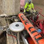
This matters more every year because slicing itself is being pushed thinner. In a 2025 review of slicing of thin semiconductor wafers, researchers describe the technology evolving toward thinner wafers and finer diamond wires precisely to feed the thin-wafer demand downstream. The same logic holds beyond silicon: compound substrates such as silicon carbide (SiC) and GaAs are thinned too, and on 200mm and 300mm production lines the slice quality still sets the ceiling. In our own experience across more than 10,000 cutting cases on diamond silicon wafer cutting wire saws, a tighter, lower-TTV slice gives the grinding and CMP steps more headroom, less material to remove, shallower damage to chase, and fewer edge defects to trim.
The practical takeaway for buyers: don’t treat slicing and thinning as separate purchasing decisions. A diamond wire saw that holds tight TTV and minimal subsurface damage, like our SiC wafer cutting saws and precision diamond wire sawsraises the ceiling on what your thinning line can achieve. For more on the upstream material side, see our guide to silicon wafer material.
Outlook: Ultra-Thin Wafers, 450 mm & Thinner-Finer Slicing

The direction of travel is set by packaging, not by wafer makers. As 3D and heterogeneous integration spread from high-bandwidth memory into mainstream logic, sub-50 µm, and increasingly sub-20 µm, die become a routine requirement rather than an exotic one. That demand is the load-bearing driver behind every change below; the broad market-growth figures often quoted (mid-single-digit annual growth for thin wafers, higher for thinning-and-dicing equipment) are directional background, not the reason fabs thin wafers. Demand is the real driver: 3D and power-device makers need sub-50 µm die, and that pull is what forces tool builders to push slicing and grinding finer.
Three shifts worth watching:
- All-dry, low-damage thinning: A 2025 study demonstrates extreme all-dry SOI wafer thinning paired with nano-TSVs, replacing wet steps to cut damage and contamination on the thinnest wafers.
- Laser and photonic debonding are scaling to handle ever-thinner dies for taller memory stacks.
- Standards keep moving: SEMI’s M1 wafer specification and 450 mm standards continue to be revised, which resets the thickness and TTV baselines buyers write into contracts.
What to do about it: when you plan a thinning roadmap for 2026 and beyond, qualify your slicing and stress-relief steps for the thinnest target you realistically need, not the thinnest the tool can reach, and lock the upstream slice quality first. For the equipment landscape, see our overview of semiconductor manufacturing equipment.
Frequently Asked Questions
Q: What does wafer thinning mean?
View Answer
Wafer thinning means reducing the thickness of a finished semiconductor wafer after its circuits are built, usually from around 775 µm down to 75–50 µm or less. The back side is ground, polished, and etched while the front-side devices are protected by a laminated tape or a bonded carrier wafer. Thinning enables 3D stacking, lower package height, better heat removal, and lower electrical losses, and it sits between slicing and dicing in the back-end flow.
Q: What is wafer backgrinding?
View Answer
Wafer backgrinding is the mechanical part of thinning, where a rotating diamond wheel removes silicon from the back of the wafer. Grinding runs in stages — coarse for speed, then fine for surface quality — and is followed by a stress-relief step such as CMP or etching.
Q: What is the typical wafer thickness?
View Answer
Standard starting thickness scales with diameter under SEMI specifications: roughly 525 µm at 100 mm, 625–675 µm at 150 mm, 725 µm at 200 mm, and 775 µm at 300 mm. After thinning, mainstream logic typically lands around 100–300 µm, while memory and 3D-stacked die go below 50 µm. Incoming thickness is fixed by the standard, but the thinned target is chosen by the device, the packaging scheme, and how much handling margin the production line can reliably hold.
Q: How thin can a silicon wafer be ground?
View Answer
Production lines routinely reach 50 µm, and advanced packaging pushes below 20 µm. The limit is handling and strength, not the grinder itself. Specialized research lines have demonstrated silicon below 10 µm.
Q: Does wafer thinning weaken the wafer or reduce die strength?
View Answer
It can, and that surprises people. Thinning by grinding leaves a subsurface damage layer of micro-cracks, and those flaws — not the reduced thickness alone — drive how easily the die fractures. Research on silicon’s subsurface damage layer confirms the damaged surface governs strength. Stress relief is the fix: removing the damaged layer with CMP, dry etch, or wet-chemical thinning measurably raises die strength. A properly stress-relieved thin wafer can be stronger than a thicker, rougher one.
Q: What’s the difference between wafer thinning and dicing?
View Answer
Thinning reduces the thickness of the whole wafer by grinding and polishing the back side. Dicing (die singulation) comes afterward and cuts the thinned wafer into individual chips by saw, laser, or stealth methods. Thinning controls how thin each die is; dicing controls how the wafer is separated into chips.
About This Analysis
We build diamond wire saws that slice silicon, SiC, and sapphire wafers, so we live one step upstream of wafer thinning. That vantage shaped this guide’s core argument, the Slice-Floor Principle, because we see daily how as-sliced TTV and subsurface damage set the headroom for every grinding and CMP step that follows. Process numbers here are drawn from published industry and academic sources; the slicing-to-thinning linkage come from our own cutting experience. Reviewed by the Shanghai Donghe Science and Technology Co., Ltd. technical team.
References & Sources
- Wafer backgrindingWikipedia (starting thickness, thinned ranges, BG tape).
- The Rise of Thin Wafer ProcessingSemiconductor Engineering, L. Peters, 2025 (precision ladder, TTV budget, bonding/debonding).
- Wafer Thinning and PolishingUniversity of Illinois, Photonic Devices Research Group (lapping, carrier handling).
- Mechanical properties of silicon in the subsurface damage layerAIP Advances (Harvard ADS).
- Progress and critical challenges in slicing of thin semiconductor wafersScienceDirect, 2025.
- Pure Ru n-TSV processing and extreme all-dry SOI wafer thinningScienceDirect, 2025.
- US10600736B2USPTO (TAIKO ring edge retention).
- SEMI Standards (M1 / 450 mm)SEMI (wafer thickness specifications).
Related Articles
- Silicon Wafer Material — what wafers are made of and how ingots are sliced.
- Semiconductor Manufacturing Process — the full sand-to-chip sequence.
- Semiconductor Manufacturing Equipment — front-end and back-end tooling.
- Types of Semiconductor Wafers — Si, SiC, sapphire, and GaN substrates.
Planning a thinning line? Start with a slice that give your grinding and CMP steps room to work. Talk to our engineers about diamond wire saws built for low-TTV, low-damage wafering.