Get in touch with DONGHE Company

Contact Form Demo

SiC Wafer Cutting Saw

SiC Wafer Cutting Saw: Diamond Wire Saw Technology For Silicon Carbide

The conveyor belt is critical in cutting precision SiC wafers in power devices’ manufacturing, due to the rising demand for third generation of semiconductors. This guide provides a compendium of information and recommendations on diamond wire saw technology such as multi-wire slicing machines, advanced cutting parameter optimization and also diamond wire loop systems. Learn how leading substrate manufacturers achieve yield rates of more than 99%, reduce awning loss (kerf) from 200µm down to under 120µm, and control subsurface damage to 4H-SiC & 6H-SiC polytypes.
35% Kerf Loss Reduction
15.2% Market CAGR
200mm Max Wafer Diameter
25m/s Wire Speed
SiC Wafer Cutting Saw Equipment

SiC Wafer Cutting Market Overview

The global silicon carbide wafer market has been witnessing tremendous growth driven by EV penetration and power electronics requirements.

Projected Market Growth (2022-2028)

$110.9M

Market Size (2022)

Global SiC Wafer Cutting Equipment
$337M

Projected (2028)

Expected Market Value
CAGR 15.2%

CAGR Growth

Annual Compound Growth Rate
75%+

PEV Market Share

SiC Demand From Electric Vehicles

What Is SiC Wafer Cutting?

Silicon carbide (SiC) wafer cutting is an integral part of semiconductor manufacturing. It includes cutting SiC ingots into thin wafer substrates. SiC is a third-generation semiconductor material. It offers very high thermal conductivity, high breakdown voltage, and high electron saturation velocity. This makes SiC a very critical material for power electronics in electric vehicles, 5G infrastructure, and in various components of the renewable energy systems.

SiC Material Properties

Silicon carbide is one of the hardest materials used in the semiconductor industry with a Mohs hardness in the range of 9.3-9.5. This requires special diamond wire saw machines with optimized parameters.
Extreme Hardness:Requires diamond abrasive tools due to its Mohs rating of 9.3-9.5
High Thermal Conductivity:3-4 times more thermally conductive than standard silicon
Wide Bandgap:4H-SiC allows for a 3.26 eV bandgap for high-temp operation
Chemical Stability:High resistance to chemical etching
Brittleness:Process with care due to low fracture toughness

SiC Cutting Challenges

SiC is exceptionally hard and brittle. Dicing rates fall to 3-10 mm/sec compared to 100-200 mm/sec for silicon, representing a bottleneck in device manufacturing economics.
High Kerf Loss:Conventional multi-wire saws cause ~200μm loss per cut
Edge Chipping:Brittle materials can experience over 20μm damage on edges
Subsurface Damage:Micro-cracks that can disrupt subsequent processing steps
Tool Wear:Quick degradation of diamond abrasives due to extreme hardness
Slow Processing:Increased cycle time that slows overall production throughput

The Role Of Wafer Cutting In Semiconductor Manufacturing

The first step in the processing of SiC after ingot growth is wafer cutting (or wafer slicing). The quality of the cut affects all following steps: grinding, lapping, polishing, or epitaxial deposition. If the cutting quality is bad, the quality of the cut can increase the time taken to process, increase the amount of material that must be removed, and decrease the yield.
1
Ingot Growth SiC boules grown via PVT method (2-3 weeks)
2
Wafer Slicing Diamond wire saw cutting into substrates
3
Grinding/Lapping Surface damage removal and flattening
4
CMP Polishing Atomic-level surface finishing
5
Epitaxy Device layer deposition

How Diamond Wire Saw Cutting Works

The diamond wire saw cutting machine has a rather simple operating principle. A continuous loop wire coated with diamond abrasive particles moves at a high speed and the SiC workpiece is fed into the wire. The diamond particles abrade the material and a precise cut with a controlled kerf width and good surface quality is achieved.

Working Principle and Mechanism

In fixed abrasive diamond wire sawing, synthetic diamond (20-60μ m) particles are electroplated onto a high tensile wire core. It is, however, unlike slurry based sawing which entails loose abrasive suspension. Some of the advantages of the fixed diamond wire include:
  • A cutting rate that is higher on average as a result of the abrasive attachment
  • Surface finishing, which is on a higher average due to surface consistency
  • A surface improvement due to uniform material removal
  • A cleaner process because of the use of a water based coolant
  • A minimal ecological footprint with respect to slurry disposal

Key Machine Components

A modern SiC wafer slicing machine contains the following essential subsystems:
🔩
Wire GuideWire alignment and spacing is maintained by precision rollers
Tension System20-60 N tension is maintained and controlled for consistency in cutting
💧
Coolant DeliveryA 6+ nozzle system is employed for thermal control
📊
Motion ControlRate and position control is set to a high degree of precision
🔄
Wire Drive10-25 m/s wire speed is achieved with the use of high speed motors
📐
WorkholdingIngot stability is achieved through secure fixturing

Diamond Wire Types and Selection

Process performance is optimized through an appropriate diamond wire selection for SiC cutting, which is determined by the following basic selection criteria.
ParameterTypical RangeImpact on Process
Wire Diameter0.1 – 0.3 mmShorter wire life = less kerf loss, whereas Longer diameter = higher wire life
Diamond Grit Size10 – 30 μ mSlower cutting = finer grit, higher surface finish
Diamond Concentration15-25%A higher concentration results in faster cutting and increased cost
Bond TypeElectroplated / ResinElectroplated for aggressive cutting, resin for a fine finish

Critical Cutting Parameters For SiC

The cutting parameters for SiC wafer must be optimized in order to achieve the desired surface quality, subsurface damage, and throughput. The combination of wire speed, feed, tension, and cooling achieve the desired process.

Wire Speed Optimization

The diamond wire speed impacts the rate of material removal and the quality of the surface. When cutting SiC, the optimum wire speeds are between 10-25 m/s. If efficiency must be increased then wire speed must be increased along with the need for increased cooling.
Wire Speed Guidelines
10-15 m/s Slower speeds allow for better surface finishing with less thermal stress
15-20 m/s Moderate speed for higher production needs
20-25 m/s Advanced cooling required for higher production

Feed Rate Control

At what rate does the workpiece advance towards the wire and begin to slice the wafer? Slower feed rates mean less stress to the material, however, cycle time is increased. When cutting SiC, feed rates of 0.1-0.5 mm/min are common with consideration to the thickness of the wafer and quality demanded.

Wire Tension Settings

Tension of the wire must be set between 20-60N to ensure cutting of the wire with no voids, deflection, or breakage. Tension must be adjusted and set through the process in order to maintain the dimensional cut and to avoid warping of the wafer.

Coolant And Lubrication Systems

Since cutting SiC generates considerable frictional heat, it is extremely important to deliver coolant effectively. Contemporary systems consist of multi-nozzle arrangements (≥ 6 jets) that spray water-based coolants at controlled temperatures. Some formulations with nano SiC additive are reported to provide better lubrication and heat transfer.

Parameter Optimization Matrix

Parameter Recommended Range Primary Impact Trade-off
Wire Speed 10-25 m/s Cutting rate, surface quality Higher speed → more heat
Feed Rate 0.1-0.5 mm/min Cycle time, SSD depth Faster feed → more damage
Wire Tension 20-60 N Cut straightness, TTV Higher tension → wire wear
Coolant Flow 6-10 L/min Temperature control More flow → higher cost
Coolant Temp 18-22°C Thermal stability Requires chiller system

Common SiC Wafer Cutting Problems We Solve

Challenges in wafer slicing due to the extreme hardness (Mohs 9.5) of Silicon Carbide. Traditional cutting methods use out dated methods that don’t satisfy the precision required by modern semiconductor manufacturers.
Excessive Kerf Loss when Slicing SiC Ingots
When diamond wire slicing is used, 200-250μm of SiC is lost with each cut, creating as much as 46% of waste during slicing of the ingots.
Subsurface Damage (SSD) Issues
When cutting parameters are not set properly to the cutting conditions, excessive subsurface damage is created and chemical mechanical polishing (CMP) that is higher in costs is required.
Decreased Speeds in Cutting SiC Wafers
Because of the extreme hardness of SiC, methods take 2-3 hours cutting a single 6 inch wafer which reduces the capacity and throughput of the production.
Heightened Rapid Wear of Diamond Wire
Because of the wire degradation due to the hardness of SiC, some wires will only cut 3,000m worth of SiC. This significantly increases the TCO due to the high cost of consumables.
Inadequate Control of Wafer Bow and TTV
Excessive wafer bow and total thickness variation (TTV) that is over 10μm occurs due to the inconsistent wire tension and thermal influences. This results in downstream processing failures.
Expanding to 200mm Wafer Production
The shift from 150mm to 200mm SiC wafers in the industry means additional investments in new pieces of equipment as the majority of current systems will not accommodate the larger, more precise cutting requirements.

Advanced Diamond Wire Saw Machine for SiC Wafer Cutting

We have developed SiC wafer cutting saw systems that incorporate innovative engineering solutions to address each and every challenge faced by leading semiconductor manufacturers.
01

Endless Diamond Wire Loop Technology

Our systems utilize proprietary endless diamond wire loop systems that eliminate wire reversal marks and achieve cutting with the same quality every time they run. In addition, the loop design decreases kerf loss to <150μm and extends wire life by 300% compared to reciprocating systems.
Result: Waste 35% less material and the wire will last 200% longer
02

Precision Wire Tension Control System

Our PLC-controlled wire tension systems, which leverage real-time load cell feedback, are the first and only systems to maintain wire tension within ±0.5N tolerance. Because tension is consistent, there is no wafer bow and TTV is <5μm on the surface of the wafer.
Result: TTV is <5μm, bow is <15μm, and warp is <20μm
03

Rocking Motion Sawing for SSD Reduction

Our patented rocking motion technology, which achieves ±12° oscillation, reduces the contact length between the wire and SiC. This way, heat and subsurface damage are minimized. This technology delivers SSD <10μm, allowing for a 50% reduction in subsequent CMP time.
Result: 8% lower sawing temperature and have <10μm SSD
04

High-Speed Multi-Wire Configuration

With up to 25m/s wire speed and optimized wire web spacing, our multi-wire diamond saw systems utilize high volume SiC production to cut multiple wafers simultaneously; thereby increasing throughput by 400% compared to single-wire cutting.
Result: Increased to 4 times throughput, <60 minutes per 6" wafer
05

6-Nozzle Advanced Coolant System

Each of the six adjustable nozzles applies precision coolant to boost uniformity in temperature, dispersion, and thermal debris. Functions with water and oil based coolant for provison of optimal cutting conditions.
Result: Uniform thermal distribution, no hot spots
06

200mm Wafer-Ready Platform

Future proof design allows for cutting of 150mm (6-inch) and 200mm (8-inch) SiC wafers with minimal changes to the equipment. A seamless upgrade path ensures your investment is protected as the industry shifts to larger wafer sizes.
Result: Investment protection, 8″ ready today

Why Use Our SiC Diamond Wire Saw Manufacturer China?

Designed for the specific challenges of SiC material processing, our fixed abrasive diamond wire saw technology is the cutting edge solution for silicon carbide wafer slicing.
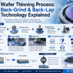
Fixed Abrasive Diamond Wire
Electroplated diamond particles (10-20μm grit) and high-tensile steel wire create superior SiC cutting performance compared to loose abrasive slurry methods.
Bosch PLC Control System
Process stability is guaranteed throughout the cutting duration with real-time parameter monitoring and adjustments with the industry-leading Bosch control system.
Minimal Kerf Loss Design
Increasing the number of wafers obtained per SiC ingot is made possible with optimized cutting geometry and wire diameter options of 0.1mm to 0.3mm.
Surface Quality Optimization
Post-processing requirements are greatly reduced with controlled cutting parameters achieving surface roughness Ra <0.5μm.
Diamond Wire Saw for SiC Cutting Machine

SiC Wafer Cutting for High-Growth Industries

Our diamond wire saw technology enables the production of SiC wafers for the fastest expanding applications in the semiconductor sector.
Power Electronics for EVs
SiC MOSFETs for high efficiency (HE) inverters, on-board chargers, and 800V battery systems for electric vehicles.
☀️
Solar Energy Systems
SiC power devices for renewable energy inverters and power optimizers for high efficiency (HE) photovoltaic systems.
📡
5G Infrastructure
SiC and GaN-on-SiC for high frequency in RF power amplifiers and base station equipment.
⚙️
Industrial Motors
SiC’s high-temperature capability in industrial motor controllers and variable frequency drives (VFDs).

Maintenance and Troubleshooting Tips for Diamond Wire Saw SiC Wafer Slicing

Preventive maintenance planning and resolution of standard issues with diamond wire saw systems

Daily Checks

Every shift
  • Coolant level
  • Wire tension
  • Filter

Service Weekly

Every 5-7 days
  • Coolant system
  • Guide roller
  • Sensor

Monthly PM

Every 30 days
  • Roller replacement
  • Motion
  • Software Updates

Quarterly Overhaul

Every 90 days
  • Calibration
  • Bearings
  • Performance

SiC Process & Cost Optimization Center

Optimize your diamond wire cutting parameters for best quality and calculate detailed cost-per-wafer breakdown for silicon carbide wafer production

Diamond Wire Cutting Parameter Optimizer

Material & Equipment Settings

Get Instant Quote
Real-time Calculation

Recommended Cutting Parameters

Wire Speed
18m/s
1025 m/s
Feed Rate
0.8mm/min
0.32.0 mm/min
Wire Tension
38N
2060 N
Rocking Angle
±10°
±0°±15°
Diamond Grit
12-15μm
825 μm
Coolant Flow
15L/min
525 L/min

Predicted Output Quality

TTV
<5μm
Excellent
Surface Ra
<0.5μm
Excellent
SSD Depth
<10μm
Good
Cycle Time
58min
Good
SiC Wafer Cutting Cost Calculator

Production Parameters

wafers/yr

Material Costs

$/ingot
wafers

Operations

$/wafer
$/hour
$
Get Instant Quote
Real-time Calculation

Cost Analysis Results

Total Cost Per Wafer
$118.50
35%
vs Traditional

Cost Breakdown

SiC Material
Ingot cost per wafer
$72.92
61.5%
Diamond Wire
Wire consumption
$22.00
18.6%
Labor
Operator time
$8.25
7.0%
Equipment Depreciation
7-year depreciation
$7.86
6.6%
Facility & Overhead
Utilities, maintenance
$7.47
6.3%

SiC Wafer Cutting Customer Case Studies

Real-world case studies demonstrating precision, yield, and cost-efficiency.

Case Study 1: Reduction of Kerf Loss by 35%

Industry EV Power Electronics
Location Germany
Wafer Size 6-inch (150mm) 4H-SiC
Duration 6 Months

Customer Background

The German automotive Tier-1 supplier is one of the largest manufacturers of SiC-based power modules for electric vehicle inverters. This company, which annually produces over 500,000 SiC MOSFET modules, is under financial stress due to the excessive raw material waste from their wafer slicing operations. This company runs 3 production lines for 6-inch 4H-SiC wafer processing for 1200V and 1700V power devices.

The Challenge

Before this project started, the customer’s multi-wire slurry saw system created unacceptable losses:

  • Kerf losses were 220μm per cut, which resulted in 38 wafers produced per 25mm of the ingot height.
  • The system wasn't economically viable as the material utilization was 52%. The SiC substrate was also costly, $800-1,200 per 6-inch wafer.
  • Extensive post-processing was required due to Sub-surface Damage (SSD) of 45-60μm.
  • Edge chipping caused device downstream yield losses due to an 8% edge chipping rate.

Our Solution

After analyzing the customer’s cutting demands, we installed a DWS-6000 Diamond Wire Saw Cutting Machine with custom features.

Machine Features
  • Wire saw diameter: 0.12mm (electroplated, 10-15μm diamond grits)
  • Wire speed: 18-22m/s (with adjustable speed for each cutting phase)
  • Feed rate: 0.3-0.5 mm/min (adaptive control in relation to cutting resistance)
  • Wire tension: 35-45N (adjustable with precision servos)
  • Coolant system: 8-zone 20±1°C water-based coolant (was adjusted during cutting)
Process Optimization
  • Entry phase optimization: The feed rate was reduced to 0.15 mm/min for the first 2mm to eliminate entry chipping.
  • Steady-state cutting: The optimum combination of wire speed and feed rate was established for the cutting.
  • Phase control on exit: Built an exit chipping prevention protocol.
  • Coolant angle optimization: Improved chip removal after adjusting the nozzle angle from 45° to 30°.

Results Achieved

Metric Before After
Kerf Loss 220μm 143μm (↓35%)
Wafers per Ingot (25mm) 38 wafers 52 wafers (↑37%)
Material Utilization 52% 71% (↑19 pts)
Subsurface Damage 45-60μm 15-25μm (↓58%)
Edge Chipping Rate 8% 1.2% (↓85%)

Business Impact

  • Annual savings on materials: €2.4 million (based on 500,000 produced wafers annually)
  • SSD depth reduction made grinding/polishing 40% less time consuming
  • 14 months to achieve ROI
  • Equipment uptime: 94% (over the 90% SLA target)
"The change from slurry sawing to diamond wire cutting was a game changer for us. The reduction of kerf loss made the investment pay off in the first year."
- Dr. Klaus Weber, VP of Manufacturing Operations

Case Study 2: Endless Diamond Wire Loop Technology

Industry Renewable Energy
Location China (Jiangsu)
Wafer Size 8-inch (200mm) 4H-SiC
Duration 8 Months

Customer Background

The customer is one of the top 3 manufacturers of solar inverters in China, with an annual production capacity of over 50GW. To bolster their vertical integration, they set up a captive SiC wafer fabrication plant. This is a strategy focused on supply chain security for the SiC MOSFETs utilized in high-efficiency string inverters. The plant works on 8-inch 4H-SiC wafers destined for 650V and 1200V devices aimed at utility-scale solar systems.

The Obstacles

The difficulties the customer faced included establishing a greenfield SiC wafer cutting operation with the following requirements:

  • Ultra-thin wafer capability: 350μm target thickness – for next-gen thin-die devices.
  • Maximum material utilization: to offset the high 8-inch SiC ingot cost (15,000+ per ingot).
  • Surface roughness Ra less than 0.3μm: to minimize the steps in processing post.
  • Single wafer cutting flexibility: for R&D prototyping and small-batch production.

Our Answer

Our recommendation is the EDW-8200 Endless Diamond Wire Loop Cutting System. It matches the user's specifications for precision cutting of SiC wafers.

Equipment Configuration
  • Endless diamond wire loop: 0.18mm diameter (brazed diamond, 8-12μm)
  • Wire loop length: 15 meters (extended life cycle)
  • Linear speed: 15-20 m/s (bidirectional oscillation mode)
  • Workpiece feed: Granite air-bearing stage (0.1μm positioning accuracy)
  • In-situ wire monitoring: Real-time wire wear detection with automatic speed compensation
Technical Execution
  1. Wire loop selection: Out of 5 wire suppliers, we selected the optimal diamond concentration and bond strength.
  2. Cutting recipe: Developed 12 cutting recipes that were customized to different ingot orientations and thicknesses.
  3. Coolant: Implemented a DI water-based coolant with custom surfactant additives.
  4. Operator training: We implemented a comprehensive training program that lasted 4 weeks and trained 8 technicians.

Results Performance Achieved

Metric Result Achieved Target / Context
Kerf Loss 0.35-0.40mm versus 0.45mm target
Minimum Wafer Thickness 300μm achieved Exceeded 350μm target
Surface Roughness (Ra) 0.22μm Exceeded 0.3μm target
TTV < 5μm Across 200mm diameter
Yield Rate (First-Pass) 96.8% -

Business Impact

  • Additional 8 wafers per ingot (from ~65 to 73 wafers per 30mm ingot section)
  • Material cost reduction: 12.3%
  • Eliminated one grinding step in post-processing, saving $8 per wafer
  • Production capacity: 3,600 wafers/month with single-shift operation
"The endless diamond wire loop technology gave us the precision we needed for thin-wafer processing while maintaining excellent material utilization. The single-wafer flexibility has been invaluable for our R&D activities."
— Wang Lei, Director of Wafer Fabrication

Case Study 3: SSD Reduction for 5G RF Device Manufacturer

Industry 5G Infrastructure
Location Japan
Wafer Size 4-inch Semi-insulating SiC
Duration 4 Months

Customer Background

Japanese semiconductor foundry in the GaN-on-SiC RF devices for 5G base stations. Their product line comprises HPAs, LNAs, and integrated MMICs for sub-6GHz and mmWave bands. The RF devices’ performance is critical, therefore demanding high-quality SiC substrates with minimal crystallographic defects.

The Challenge

The primary concern from the customer included the subsurface damage which affected the quality of the GaN epitaxial growth:

  • Damage depth exceeding 40μm: this causes threading dislocation propagation into GaN epilayer.
  • Concentration of residual stress: this resulted in issues with wafer bow during epitaxy (exceeding 30μm bow on 4-inch wafers).
  • Substrate induced defects: resulted in an RF device failure rate of 4.2%.
  • High crystal orientation required: ± 0.1° for optimum GaN growth.

The Solutions

For this we utilized the DWS-4100P Precision Diamond Wire Saw fully configured with specialized features for SSD-reduction.

Equipment Configuration
  • Ultra-fine diamond wire: 0.08 mm (precision electroplated, 5-8μm diamond grit).
  • High-speed cutting: 25-30m/s wire speed (in order to reduce unit cutting force).
  • Ultra-low feed rate: 0.08-0.15mm/min (to minimize mechanical stress).
  • Goniometer with precision stage: ±0.01° (for off-axis cutting).
  • SSD in Real-Time: Acoustic Emission Sensors for Artificial Intelligence surveillance.
Process Innovation
  1. Multi-phase cutting protocol: Implemented 3-phase cutting (rough → semi-finish → finish) with fine parameters for each step.
  2. Stress-relief cooling: Developed a proprietary coolant with stress-corrosion inhibiting additives.
  3. Integrated SAM verification: Integrated SAM (Scanned Acoustic Microscopy) for 100% inspection of SSD.
  4. XRD Guided Orientation: Used X-ray Diffraction for ±0.05° Alignment pre-cutting.

Results Achieved

Metric Before After
Subsurface Damage Depth 40-55μm 8-12μm (↓78%)
Wafer Bow (4-inch) >30μm <8μm (↓73%)
Crystal Orientation Accuracy ±0.15° ±0.05° (↑3x precision)
RF Device Failure Rate 4.2% 1.1% (↓74%)
GaN Epi Defect Density 5×10⁵ cm⁻² 8×10⁴ cm⁻² (↓84%)

Wafer Epitaxy and Substrate Quality Improvement

  • Annual yield improvement value: ¥180 million (fewer device failures)
  • Grinding/polishing time reduced by 55% (from 45 min to 20 min per wafer)
  • Customer product reliability improved – qualifying for Tier-1 base station OEMs
  • Now processing 6-inch wafers – second machine ordered for capacity expansion
"The dramatic reduction in subsurface damage has been game-changing for our GaN epitaxy quality. We've seen direct correlation between improved substrate quality and RF device performance."
— Dr. Tanaka Hiroshi, CTO

Frequently Asked Questions (FAQs)

Q: What exactly is an SiC wafer cutting saw?
A: An SiC wafer cutting saw is a machine that uses a diamond wire saw to cut silicon carbide ingots into thin wafer substrates. The wire saw is coated in diamonds and cuts at a speed of 10 to 25 meters per second. This speed, coupled with coolant systems and tension control, allows for the cutting of SiC's extreme hardness, which ranks at Mohs 9.5.
Q: Why diamond wire saw and not something else for cutting SiC Wafers?
A: Utilizing a diamond wire saw to cut silicon carbide is the best option because of the extreme toughness of SiC. This toughness makes the use of metal blades impractical, as nothing else can cut effectively and in a time efficient manner, all while achieving a good surface finish, than diamond abrasives. Furthermore, dedicated SiC wafer cutting saws have reinforced and cooled structures to deal with the extreme applications.
Q: How much kerf loss do SiC wafer cutting saws have?
A: When cutting SiC with diamond wire saws, the common kerf loss that can be expected is 180–220µm. Some advanced SiC wafer cutting saws that use ultra-fine wire with a precision tension control can reduce kerf loss to 100–150µm. This saves approximately 2–3 wafers per ingot and increases the material utilization significantly.
Q: What wire speed is best for SiC wafer cutting saws?
A: SiC wafer cutting saws are most effective between 10 and 25 meters per second. Surface finishing is better at the lower end of the range (10 to 15 meters per second), while the higher end (20 to 25 meters per second) improves throughput, but requires better cooling systems. For balanced SiC production, the majority of diamond wire saw cutting machines are set to 15 to 20 meters per second.
Q: How do I reduce edge chipping on my SiC wafer cutting saw?
A: To reduce edge chipping on diamond wire saw cutting machines, you should slow the feed rate at the cut entry and exit; adjust the coolant nozzle to ensure proper cooling; keep wire tension steady (between 25 and 40 Newtons); and select an appropriate diamond grit (15 to 20 microns). Also, regularly inspect the guide rollers, as uneven cutting forces that cause chipping can be a result of guide roller malfunction.
Q: What's the difference between multi-wire and single-wire SiC wafer cutting saws?
A: Multi-wire diamond wire saw cutting machines are optimal for high-volume production of SiC wafers as they can cut whole ingots at once using hundreds of wires in parallel. Single-wire SiC wafer cutting saws are lower in capital cost and flexibly accommodate cropping, research and development, and sample preparation. Single-wire saws can also offer the potential for tighter kerf capability, and often lower cost.
Q: What type of maintenance is done on a SiC wafer cutting saw?
A: Daily coolant inspections and tension adjustment are needed on SiC wafer cutting saws, while guide rollers are inspected weekly, and alignment is checked monthly; calibrations are done every quarter. SiC wafer production showed that maintaining diamond wire saw cutting machines resulted in consistent cutting quality, minimized unforeseen downtimes, and increased the operational lifespan of the machines.
Q: Are there other materials that can be cut on the diamond wire saw cutting machines besides SiC wafers?
A: Typically, machines for diamond wire saw cutting that are intended for SiC can also cut sapphire, silicon, GaN, quartz, and ceramics. With the adjustment of the cutting parameters, the SiC wafer cutting saw which is able to cut the hardest materials, handles other materials that are also hard because SiC is the most demanding application.
Q: What is the price range of SiC wafer cutting saws?
A: From $50,000 to $150,000 are the price ranges for single-wire SiC wafer cutting saws and for production multi-wire diamond-wire saw cutting machines the price range is $200,000 to $500,000. More sophisticated automated systems are of extra costs that range over $500,000. Other expenses such as diamond wire ($5-15 for every wafer), maintenance, and coolant are added, which makes the costs considerable.
Q: What is the ROI of a SiC wafer cutting saw?
A: ROI for diamond wire saw cutting machines in SiC production typically achieves payback within 3-6 months. Kerf loss reduction of up to 35% translates to a $50-200 per wafer reduction in material costs. Additionally, improved yield from better edge quality and subsurface damage further accelerates SiC wafer cutting saw screw ROI.