Get in touch with DONGHE Company
-
Phone: +86 181-1645-5490
-
Email: Sales18@DongheScience.com

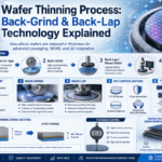
Semiconductor Manufacturing: Wire Saw in Wafer Production
Wire Saw Technology in Semiconductor Wafer Production: A Comprehensive Guide
Exploring the Critical Role of Precision Cutting in Modern Electronics Manufacturing
The production of semiconductor wafers represents one of the most intricate and sensitive processes in modern electronics manufacturing. At the heart of this process lies wire saw technology, a critical innovation that transforms silicon ingots into the ultra-thin wafers that form the foundation of virtually every electronic device. This comprehensive examination explores the operational principles, technological advancements, and transformative impact of wire saw technology in meeting the rigorous demands of today’s semiconductor industry.
The Role of Wire Saws in the Semiconductor Industry

Wire saws have established themselves as indispensable instruments in semiconductor manufacturing, enabling the precise and efficient cutting of semiconductor materials such as silicon into wafer-thin slices. These wafers serve as the fundamental building blocks for electronic chips utilized across countless technologies. The wire sawing process minimizes material loss, delivers exceptional cutting accuracy, and produces wafers with consistent thickness—all critical factors that modern semiconductor manufacturing demands to meet increasingly stringent quality specifications.
Introduction to Wire Saw Technology
Wire saw technology employs a precision cutting technique utilizing thin wire coated with abrasive materials to slice through substrates with exceptional accuracy. This methodology has become standard practice in semiconductor manufacturing, facilitating mass production of silicon wafers while minimizing raw material waste.
The wire maintains constant tension throughout operation, and the application of either abrasive slurry or fixed-abrasive wire ensures consistent cutting results. Wire saws produce wafers with uniform thickness and excellent surface quality—both essential requirements for the performance and reliability of modern electronic components. This technology forms the backbone of advanced microfabrication processes throughout the electronics industry.
Key Advantages of Wire Saws in Wafer Production

Wire saw technology delivers multiple critical benefits that establish it as the preferred method for wafer production. The following advantages demonstrate why this technology has become indispensable in modern semiconductor manufacturing:
1
High Material Utilization Efficiency
Wire saws deliver exceptional precision, resulting in minimal material loss during the cutting process. This proves particularly critical when working with expensive materials such as silicon, sapphire, and gallium arsenide. Research demonstrates that cutting-edge wire saws achieve material utilization rates of 95% or higher in optimal conditions.
2
Uniform Wafer Thickness
The consistent tension applied to the wire produces highly uniform cutting results, yielding wafers with exceptional thickness consistency. This uniformity proves essential for semiconductor applications, as even minor thickness variations can significantly impact device characteristics and overall performance.
3
Superior Surface Quality
Wire saws produce wafers with minimal surface roughness, significantly reducing the need for extensive post-processing. Advanced systems can achieve surface quality measurements of 0.1 µm Ra, substantially decreasing both time and cost requirements for finishing processes following the initial cut.
4
Scalability for Mass Production
Wire saws excel at producing large volumes while maintaining consistent quality standards. The process accommodates multiple wafers simultaneously, dramatically increasing throughput and meeting the substantial production demands of both semiconductor and solar cell industries.
5
Adaptability to Advanced Materials
Modern wire saws handle a diverse range of materials, including exceptionally hard and challenging substrates such as silicon carbide (SiC) and gallium nitride (GaN). This versatility ensures wire saws remain essential for manufacturing advanced power electronics and optoelectronic devices.
These combined advantages establish wire saws as the predominant technology in wafer fabrication, directly influencing both the cost efficiency and quality standards of final electronic components.
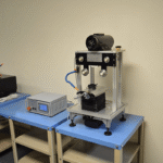
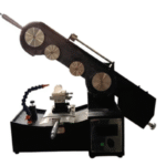
Wire Saw Cutting Techniques

Wire saw cutting methodologies employ thin, abrasive-coated wire moving at high velocity to achieve precise material separation. The two primary approaches include multi-wire sawing and single-wire sawing, each optimized for specific applications and production requirements.
- Multi-Wire Sawing: Utilizes multiple parallel wires to dramatically increase production throughput for mass manufacturing applications. This approach enables simultaneous processing of numerous wafers, significantly reducing per-unit production time.
- Single-Wire Sawing: Primarily employed for prototype development or specialized cutting requirements where precision takes precedence over volume. This method offers enhanced control for experimental or custom applications.
Both methodologies depend on precise control of tension, wire speed, and slurry or abrasive application to achieve clean cuts with minimal material loss. The accuracy and versatility of these techniques have proven particularly valuable when cutting brittle or hard materials without inducing structural damage.
Understanding Silicon Wafer Production

What is a Silicon Wafer?
A silicon wafer consists of an extremely thin, flat piece of crystalline silicon serving as the primary substrate for manufacturing integrated circuits and other microelectronic devices. These wafers undergo precision manufacturing to ensure dimensional accuracy, thickness uniformity, and defect minimization—all factors directly influencing semiconductor component performance and reliability.
Silicon wafers have become the predominant substrate choice in high-technology industries due to silicon’s semiconductor properties, abundant availability, and ability to withstand manufacturing process temperatures. Applications range from computer processors and memory devices to solar cells and sensors. Wafer diameters have evolved continuously, currently ranging from 50 mm to over 300 mm, driving increased productivity and reduced costs through enhanced manufacturing efficiency.
Monocrystalline Silicon vs. Multicrystalline Silicon
The fundamental distinction between monocrystalline and multicrystalline silicon lies in their crystal structure, manufacturing process, and resulting performance characteristics. The following comparison highlights key differences:
Processes Involved in Wafer Manufacturing
Wafer manufacturing, essential for producing photovoltaic cells and semiconductor components, encompasses a series of complex and carefully controlled processes. The Czochralski (CZ) technique serves as the primary method for producing monocrystalline wafers, while the casting method addresses multicrystalline wafer production.
1. Production of Ingots
Monocrystalline Process:
The process begins with melting high-purity silicon using the Czochralski method. A seed crystal is dipped into the molten silicon and slowly rotated while being gradually withdrawn. This controlled process produces a cylindrical ingot with perfect crystal alignment throughout its structure.
Multicrystalline Process:
Silicon is melted and then cooled to solidify within a block formation, resulting in multiple crystal orientations. While this process operates faster than the monocrystalline method, the trade-off involves reduced crystal purity and uniformity.
2. Sawing the Ingots
Precision wire saws transform monocrystalline ingots or multicrystalline silicon blocks into individual wafers. Thickness control proves critical both for material conservation and maintaining structural integrity throughout subsequent processing stages.
3. Surface Treatment
Following the cutting process, wafers undergo cleaning, texturing, and chemical etching to eliminate surface defects created during sawing. Monocrystalline wafers typically receive micro-pyramid texturing to enhance light trapping capabilities, while multicrystalline wafers may undergo isotropic etching for improved uniformity.
4. Doping
Wafers are placed in controlled environments where specific dopants—such as phosphorus or boron—are diffused into their surfaces, creating a p-n junction. This step proves fundamental in determining the wafer’s semiconductor behavior and electrical characteristics.
5. Anti-reflective Coating
A thin anti-reflective coating layer is applied to wafer surfaces, enhancing their ability to absorb sunlight by reducing light reflection. Silicon nitride commonly serves as the preferred material for this application.
6. Quality Inspection
The final manufacturing stage involves comprehensive quality control assessments examining wafer dimensions, thickness, surface quality, and electrical properties against industry standards. Wafers failing to meet specifications are either recycled or properly disposed of according to environmental protocols.
These interconnected processes collectively produce high-quality wafers essential for the performance and reliability of solar photovoltaic systems and semiconductor devices.
Advancements in Diamond Wire Saw Technology

Recent innovations in diamond wire saw technology have dramatically enhanced the precision and efficiency of wafer slicing processes. Modern wire saws now achieve thinner cuts with substantially reduced material loss, effectively minimizing kerf waste and improving overall material utilization. Advanced wire coatings combined with innovative diamond particle distribution have significantly increased both durability and cutting performance, extending operational lifespans while reducing replacement costs.
State-of-the-Art Diamond Wire Innovations
Contemporary diamond wire technology development has fundamentally transformed cutting applications in terms of precision and energy efficiency. The integration of ultra-fine diamond grains with enhanced wire tension systems has yielded substantial improvements in cutting accuracy while simultaneously reducing material wastage.
Additionally, enhanced automation and monitoring systems now enable real-time process optimization and consistent cutting quality maintenance. These combined innovations contribute to higher production yields, reduced operational costs, and improved sustainability throughout wafer manufacturing processes.
Precision Wire Saws: Features and Benefits
Unmatched Cutting Accuracy
Diamond wire saws operate under high tension utilizing ultra-fine abrasive particles to achieve extremely precise cuts. These systems maintain tolerances as tight as ±0.01 mm, making them ideal for applications requiring exceptional precision, such as semiconductor wafer slicing.
Negligible Material Loss
Advanced wire tension systems and optimized cutting speed parameters ensure kerf loss remains below 10%. This achievement maximizes usable material yield while significantly reducing manufacturing costs associated with raw material procurement.
Application to Diverse Materials
Precision wire saws successfully process materials ranging from extremely hard substrates like silicon carbide to delicate materials such as sapphire and quartz. This versatility establishes them as essential technology across sectors spanning electronics to optics.
Enhanced Production Efficiency
Continuous automation and advanced surveillance systems integrated into modern precision wire saws minimize downtime while maximizing throughput. These systems demonstrate 20-30% higher production efficiency compared to conventional cutting methodologies.
Longer Wire Lifespan
Implementation of advanced wire coating technologies and improved wire-recycling processes has extended cutting wire lifetime, reducing replacement requirements by up to 40%. This advancement delivers substantial cost savings while enhancing overall production workflow sustainability.
Comparison with Traditional Cutting Methods
When evaluating efficiency, accuracy, and sustainability metrics, precision wire saws demonstrate substantial advantages over traditional approaches such as abrasive saws and manual mechanical cutting. Conventional systems frequently encounter challenges including excessive material wastage, cutting inaccuracies, and extended downtime due to maintenance requirements.
15-20%
Traditional Method Material Loss
<5%
Precision Wire Saw Material Loss
Research demonstrates that traditional methods average 15-20% material loss, while precision wire saws reduce this figure to less than 5%.
Furthermore, wire recycling systems and enhanced wire durability translate to lower long-term operational costs for manufacturers. Precision wire saws equipped with wire recycling and reconditioning systems avoid losses associated with frequent wire replacement, maintaining uninterrupted production activities. Recent operational data indicates traditional systems demonstrate approximately 25% lower throughput efficiency compared to precision wire saws, highlighting the compelling performance advantages of transitioning to modern wire saw technology in industrial applications.
Efficiency and Precision in Semiconductor Manufacturing

Contemporary wire saw technology has revolutionized semiconductor production by ensuring minimal material waste and exceptional cutting precision, establishing both environmental sustainability and cost-effectiveness as achievable goals. Advanced systems maintain kerf loss at minimal levels, maximizing usable wafer yield from each substrate. The superior cutting precision produces wafers with consistent thickness and surface quality—critical factors for high-performance semiconductor applications.
Impact of Wire Saw Cutting on Surface Quality
Wire saw cutting significantly influences substrate surface quality across both semiconductor and photovoltaic industries. Surface quality impact manifests through several crucial parameters, each playing an essential role in final product performance and subsequent processing requirements.
Surface Roughness (Ra)
The wire sawing process generates micrometer-level surface irregularities on substrate surfaces. Advancements in wire materials and cutting speed optimization can reduce roughness to minimum values of 0.5 µm Ra under ideal operating conditions.
Subsurface Damage (SSD)
Subsurface layer damage results from the interaction between cutting wire force, speed, and material properties. Advanced cutting methodologies have reduced SSD to below 10 µm on silicon wafers, substantially minimizing post-cutting processing requirements.
Kerf Width Uniformity
Precision wire saw operation ensures consistent kerf width throughout the cutting process, producing substrates with uniform thickness. Variations typically remain within ±5 µm tolerance, reducing material waste and enhancing downstream processing accuracy.
Surface Contamination
Wafer surfaces may experience contamination from particles and cutting agents during processing. Proper slurry management combined with effective cleaning systems achieves minimal contamination levels, delivering surfaces with reduced chemical residue presence.
Edge Chipping
Edge integrity proves crucial for substrate durability and mechanical reliability. Advanced tension control systems employed by modern wire saws limit edge chipping to less than 2%, preventing crack propagation during shipping and subsequent processing operations.
Careful technological implementation in wire saw design and process parameter optimization has significantly improved surface quality across these factors, consistently meeting stringent industry standards.
Kerf Reduction and Material Savings
Kerf reduction represents a primary advantage delivering enhanced material utilization and substantial cost savings. Among various cutting technologies, wire saws demonstrate the most progressive approach through continuous improvements that minimize material loss during processing. Reduced cutting width translates directly to decreased waste and improved output efficiency.
Optimal kerf dimensions remain achievable through deployment of thinner wires combined with precisely tuned cutting parameters, maintaining superior accuracy while reducing operational costs. This optimization effectively addresses both industrial production requirements and economic sustainability objectives.
Enhancements in Cutting Process for Hard and Brittle Materials
Processing hard and brittle materials has advanced through precision engineering integration with data-driven optimization approaches, establishing new performance benchmarks. Laser-assisted cutting and ultrasonic machining have gained prominence as preferred methodologies, offering minimal material damage when processing silicon, ceramics, or glass substrates.
These techniques address brittle substrate challenges—including crack formation and chipping—through precisely controlled energy and force application. Dynamic cutting parameter regulation increasingly benefits from machine learning applications, optimizing variables such as wire tension, cutting speed, and cooling fluid flow in real-time.
This approach extends tool lifespan, reduces downtime, and enhances processing reliability. Utilization of high-performance computational models for predicting material behavior during cutting provides manufacturers with unprecedented accuracy while achieving cost optimization. This precise calibration ensures processing techniques remain robust and capable of evolving alongside advancing high-technology material requirements.
Recommend reading: Hard and Brittle Material Cutting Wire Saw | Precision Diamond Wire Saw Machine
Frequently Asked Questions
What is the primary function of a wire saw in the semiconductor production process?
A wire saw serves as a specialized cutting apparatus designed exclusively for slicing silicon wafers—the foundational material for producing integrated circuits, transistors, and other semiconductor devices. The cutting mechanism employs a thin steel wire rotating at high velocity, often combined with abrasive slurry or diamond-impregnated wire for material removal. This methodology enables manufacturers to slice hard, brittle materials including silicon, silicon carbide (SiC), and sapphire with exceptional precision.
What are the main differences between wire slicing and conventional blade cutting?
Conventional blade cutting methods, such as inner diameter (ID) sawing, process individual wafers sequentially using rigid blade systems. Contemporary multi-wire cutting machines operate through multiple parallel wires simultaneously processing material. Each wire contributes to slicing a single ingot into hundreds of wafers in one pass. This fundamental difference yields dramatically increased throughput while reducing material loss (kerf loss) between wafers compared to traditional blade technologies.
What are the advantages of wire saws in wafer making?
Wire saws deliver numerous significant benefits in semiconductor production:
- High Throughput: Simultaneous processing of hundreds of wafers dramatically reduces per-wafer production time.
- Reduced Kerf Loss: Extremely fine wires (often 100 microns or less) minimize precious silicon conversion to waste during cutting.
- Superior Surface Quality: Wire saw cutting generally inflicts less subsurface damage and mechanical stress compared to rigid blade cutting, resulting in improved uniformity and reduced breakage rates.
- Flexibility: This methodology readily accommodates larger ingot diameters (300mm and 450mm) prevalent in contemporary manufacturing, which traditional blade systems process less efficiently.
What is the distinction between slurry and diamond wire sawing?
Slurry-based sawing employs bare steel wire carrying loose abrasive slurry (combining oil or glycol with silicon carbide particles) to the cutting zone. Abrasive particles achieve material removal through rolling action, gradually wearing away silicon.
Diamond wire sawing (DWS) utilizes wire with diamond particles directly bonded to its surface through electroplating or resin bonding methods. DWS achieves material removal through scratching or grinding action rather than rolling abrasion. DWS demonstrates faster operation, cleaner processing, and enhanced environmental sustainability by eliminating slurry waste concerns.
What are the downsides of wire sawing technology?
Despite its substantial advantages, wire sawing presents several technical challenges:
- Wire Breakage: Wire failure during cutting can destroy entire ingots and halt production processes, resulting in significant financial losses.
- Surface Defects: Improper wire tension or speed settings may create saw marks, waviness, or thickness variations (TTV) across wafers, requiring extensive polishing correction.
- Thermal Management: Cutting operations generate substantial heat, necessitating proper cooling systems to prevent thermal wafer warping or wire deterioration.
How has wire saw technology improved in recent years?
Recent improvements focus on enhancing efficiency and reducing operational costs. The industry has predominantly transitioned to diamond wire sawing for silicon wafer production, driven by its superior speed and reduced waste profile. Additionally, manufacturers continue reducing wire diameters, further minimizing kerf loss. Advanced automation and real-time monitoring systems now enable operators to detect tension abnormalities or potential wire breaks before escalation to complete failure, ensuring higher production yield quality and consistency.