Get in touch with DONGHE Company
-
Phone: +86 181-1645-5490
-
Email: Sales18@DongheScience.com

Diamond Wire Saw for Silicon Wafer: Technical Guide

The production of silicon wafers represents a major step in the semiconductor industry, where precision and efficiency play the most important roles. The diamond wire saw, a high-tech tool used in this area, has become the main technical advancement in the method of handling and cutting silicon wafers.
Purpose of This Guide: Whether you are a specialist in the manufacturing field or an engineer looking for process optimization, this guide will show how diamond wire saws contribute to precision, material waste reduction, and operational efficiency in semiconductor technology.
Introduction to Silicon Wafer Dicing
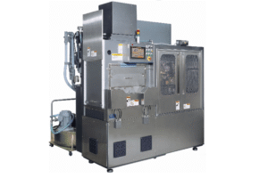
Wafer dicing of silicon is an essential procedure in semiconductor manufacturing, wherein silicon wafers are accurately sliced into separate chips or dies. This action is necessary to pack the wafers and incorporate them into electronic devices.
The procedure often uses instruments like diamond saws or laser dicing systems and gives top priority to precision that can prevent the destruction of fragile circuits. The most important factors are reducing kerf loss, managing edge chipping, and having enough throughput to satisfy industry requirements.
What is a Silicon Wafer?
The silicon wafer is a thin and smooth disc of extremely purified silicon that functions as the main substrate for making integrated circuits and other microelectronics. Due to its semiconductor characteristics, silicon can efficiently control as well as conduct electrical currents, making it indispensable in modern electronics.
Manufacturing Process Overview:
- Wafers are obtained through a complicated process beginning with the melting of high-purity silicon
- Growing of a cylindrical crystal using the Czochralski method
- Crystal is cut into thin wafers with specific thickness and surface quality using accurate techniques
- Wafers undergo rigorous cleaning, polishing, and sometimes doping processes
- Available in standard sizes, typically from 100mm to 300mm in diameter
Importance of Wafer Dicing in Semiconductor Manufacturing

Wafer dicing is a critical phase in semiconductor manufacturing, consisting of very accurately cutting up silicon wafers into dies or chips. This process keeps semiconductor devices intact and working while reducing waste and defects to a great extent.
1. Precision and Accuracy
Wafer dicing ensures the alignment of microelectronic components and cutting of chips with utmost precision. Advanced dicing techniques can achieve accuracy within a few microns, allowing for high-performance devices even when features are packed very closely together.
2. Reduction of Material Waste
Using cutting methods such as laser dicing or stealth dicing, manufacturers can cut down on kerf losses considerably. This maximizes the usage of precious silicon wafers, making the process more cost-efficient.
3. Minimization of Defects
The dicing process employs techniques that counteract mechanical stress, edge chipping, and contamination. Protective coatings or plasma dicing ensure that fine structures formed during earlier processing stages remain undisturbed.
4. Scalability for Mass Production
Wafer dicing methods are designed to be scalable for large-scale production. Automated dicing saws together with AI-controlled quality assurance systems enable uninterrupted production rates matching precision cutting requirements.
5. Adaptability to Emerging Technologies
High-tech applications like 5G, IoT, and AI require smaller and more intricate chips. Wafer dicing continues to evolve, providing solutions for thinner wafers and advanced packaging techniques like 3D stacking.
Understanding Diamond Wire Saw Technology
Diamond wire saw technology is a modern method mainly used for cutting hard materials such as semiconductor wafers, silicon, and crystals with precision and efficiency. The process includes a thin wire embedded with artificial diamonds that cuts through materials abrasively with minimal waste and high accuracy.
What is a Diamond Wire Saw?
A diamond wire saw is a cutting-edge tool that cuts materials using a wire embedded with diamond particles (either synthetic or natural), enabling very precise material removal. The working principle involves moving the diamond-coated wire in a controlled manner, thus cutting through hard materials with remarkable accuracy.
Key Components:
- Wire Material: Typically made of steel or other strong alloys, guaranteeing long life and ability to withstand tension without breaking
- Diamond Particles: Enable the wire to pierce through even the hardest materials with little thermal impact, preventing unintentional damage or deformation
- Applications: Extensive use in semiconductor production, solar cell manufacturing, and geological survey where precision, minimal waste, and perfect finish are essential
Benefits of Using Diamond Wire Saws for Silicon Wafer Cutting

| Benefit | Description | Key Data |
|---|---|---|
| Enhanced Precision | Ultra-precise cutting producing silicon wafers with very small dimensional deviations | Kerf widths as tiny as 120 micrometers (μm) |
| Reduced Material Wastage | Thin wire design results in minimal kerf loss during cutting process | ~50% less wastage vs. slurry-based methods |
| Improved Surface Finish | Creates exceptionally smooth surface finish, reducing post-processing needs | Surface roughness < Ra 0.5 μm |
| Higher Cutting Speed | Advanced diamond-coated wire enables faster cutting than traditional methods | Cutting speeds > 1 m/s achievable |
| Lower Environmental Impact | Eliminates abrasive slurry use and reduces power consumption | Less contamination, simpler waste disposal |
The Wafer Dicing Process
The wafer dicing process involves cutting semiconductor wafers into individual chips or dies. This procedure typically uses highly accurate mechanical sawing or laser ablation, guaranteeing minimal damage to delicate material.
Preparation of Silicon Wafers for Dicing
Preparation of silicon wafers for dicing is a precisely controlled method to ensure the best results when cutting wafers into separate dies. Wafers must be cleaned before dicing to remove impurities like particles, organic residues, or chemical films that might impair cutting accuracy or damage the substrate.
Preparation Steps:
- Cleaning: Use of ultrasonic baths, chemical solutions, or advanced plasma treatments depending on application requirements
- Protective Layer Application: Application of photoresist or oxide films to protect delicate areas during handling and cutting
- Inspection: Examination for structural flaws or topographical non-uniformities using atomic force microscopy (AFM) or optical scanners
- Real-Time Monitoring: Smart metrology platforms incorporating machine learning algorithms predict and flag potential slicing problems before the process starts
Stages of the Wafer Dicing Process
Stage 1: Wafer Mounting
The wafer is attached to a dicing tape that is then mounted to a frame, providing stability during the entire procedure.
Stage 2: Alignment and Inspection
The wafer is precisely positioned using high-tech optical systems and examined for any flaws or irregularities that might affect dicing quality.
Stage 3: Scribing or Laser Grooving
If necessary, scribing or laser grooving marks the dicing paths with thin grooves.
Stage 4: Dicing
Using diamond or laser tools, the wafer is cut into distinct dies exactly as planned through the dicing process.
Stage 5: Cleaning and Die Inspection
The wafer is cleaned to remove any dust generated during dicing, and individual dies are inspected for quality prior to packaging.
Challenges in Wafer Dicing
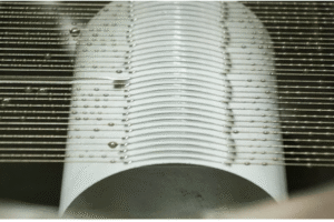
Wafer dicing presents various major difficulties that affect precision, efficiency, and overall output. Understanding these challenges is critical for process optimization.
Common Wafer Dicing Challenges
| Challenge | Description | Solution |
|---|---|---|
| Mechanical Stress | Control of stress during cutting that may result in micro-cracks or defects | Adoption of laser dicing with femtosecond lasers |
| Complex Designs | Finer geometries and thinner wafers increase risk of damage or contamination | Use protective coatings and advanced monitoring |
| Temperature Control | Heat increase during dicing reduces material integrity if not controlled | High-pressure deionized water cooling systems |
| Process Accuracy | Maintaining precision while scaling for high-volume production | Real-time monitoring systems and robotics |
Impact of Material Properties on Dicing Performance
Material properties play a major role in determining the efficiency, quality, and precision of the wafer dicing process. Variations in properties directly influence tool wear, cut uniformity, and wafer integrity.
Hardness
Directly influences material’s abrasiveness against the dicing blade. Hard materials like silicon carbide cause faster blade wear, requiring frequent replacement or more robust tooling.
Fracture Toughness
Determines how far material can resist crack propagation. Low toughness materials may suffer from chipping or microcracking at edges, negatively affecting yield.
Thermal Conductivity
Low conductivity materials suffer from thermal stress due to localized heating. Heat-affected zones or thermal deformation may cause structural integrity loss.
Crystal Orientation
Crystalline structure orientation greatly affects the cutting path. Misalignment with crystal direction increases mechanical resistance, causing chipping or uneven cuts.
Porosity
Determines structural uniformity and behavior under mechanical stress. High porosity causes irregular tool engagement, leading to uneven cuts and reduced accuracy.
How to Overcome Dicing-Related Limitations
To properly mitigate limitations of the dicing process, specific data-oriented measures are necessary. Below are comprehensive strategies for fighting dicing problems.
1. Perfect the Choice of Blade
The proper type and grade of blade are essential. Diamond blades with the right grit size and suitable bonding help in cutting down material efficiently.
Key Data: Application of resin-bonded blades to brittle wafers improves cutting with up to 30% reduction in chip formation frequency while extending blade useful life.
2. Regulate Cutting Speed and Feed Rate
Proper spindle rotational velocity and feed velocity depending on material hardness and thickness minimizes vibration patterns and tool breaking.
Key Data: For brittle materials like silicon, spindle speed over 30,000 RPM and feed rate less than 20 mm/second maintains sharp cutting edges.
3. Adopt Advanced Cooling Systems
Proper employment of coolants assists in overheating and wear debris troubles, leading to reduced surface wear.
Key Data: Installation of high-pressure deionized water systems reduces thermal stress, enhancing about 25% cleaner cuts.
4. Integrate Laser Dicing Method
Thin wafers and difficult materials promote the use of laser technology, which offers better results in such cases.
Key Data: A 40% decrease in wafer defects for wafers less than 50 microns thickness when comparing conventional cutting to laser cutting.
5. Blade Dressing and Tools Inspection
Maintaining tool integrity over time is aided by scheduled blade dressing and inspection of tools.
Key Data: Preventative maintenance system coupled with online monitoring extends tool useful life by 20% while reducing maintenance downtime.
Advanced Cutting Techniques
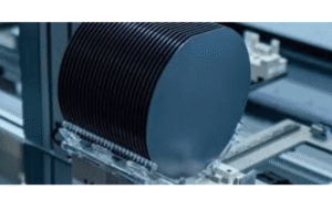
Several advanced techniques have emerged to address the shortcomings of existing process methods and enable accurate and cost-efficient manufacturing in various industrial applications.
Stealth Dicing
Stealth dicing is a technique that uses a special multipoint laser beam to manipulate the subsurface area of the object with laser energy and create subsurface modification along cutting edges. This approach eliminates reliance on abrasives, meaning cuts are cleaner and particle contamination is minimal.
Advantages of Stealth Dicing:
- Ensures geometry of materials is saved, especially for thin or easily breakable wafers
- Eliminates physical contact and abrasive-treated techniques
- Makes cracks, chipping, and distortions reach their bare minimum
- Particularly useful for thin and brittle high-cost materials
Laser Dicing
Laser dicing is a proficient technique in transforming material, which unlike physical forces, uses laser beams effortlessly and speedily. This method is viable when brittle materials are involved such as in cutting semiconductors and ceramics.
Laser-assisted dicing incorporates tools that apply heat in concentrated points resulting in micro-cracking of the region at the point of cutting without use of any physical tools, hence reasonably reducing mechanical stress and leading to fewer chances of chipping effects on the workpiece.
Plasma Dicing
Chemical plasma dicing is a relatively new technique for removing material with electric discharge or plasma. This technique is very useful in extreme cases where there is a need for very thin wafers and very tight tolerances.
Plasma dicing achieves better edge quality and precision, improves the strength of the dies, and ensures essential functioning of devices when comparing to abrasive blade dicing that is used for most historical silicon wafer cutting applications.
High Efficiency Silicon Cutting Techniques

When cutting monocrystalline silicon, more care should be taken to maintain the structure of the material and its performance characteristics. The following are main techniques that can assist in improving the process while minimizing material usage and wastage.
| Technique | Description | Performance Data |
|---|---|---|
| Laser Stealth Dicing | Focuses laser beam inside the wafer, completely eradicating inherent stresses of mechanical removal | Raises yield rate up to 20% for thin wafers <200 micrometers |
| Diamond Wire Sawing | Uses fine wire coated with diamond to cut silicon ingot into very thin slices with minimal wastage | Reduces kerf loss below 100 μm per cut, greatly increasing material utilization |
| Plasma Dicing | Uses specially designed etch that physically reprocesses silicon wafer without contact | Achieves edge roughness <1 μm, applicable to advanced microelectronics |
| High-Frequency Blade Cutter | Combines high-frequency ultrasonic cutter blade to reduce friction and heat | Increases cutting speed by 30-40% compared to mechanical means |
| Cleave and Polish Technique | Physical process involving scoring wafer in crystallographic directions, then cleaving and polishing | Provides ultra-thin damage layers with surface roughness reduction below 10 nm |
Important Note: All methods mentioned cover different aspects of silicon wafer cutting technology, but use is limited by application constraints on wafer thickness, design geometry, and productivity requirements.
Best Practices for Effective Wafer Dicing
To ensure high quality and reduce wastage during semiconductor production, wafers should be diced effectively. The following actionable guidelines aim at improving the process of dicing with thorough explanations and statistics.
Best Practice #1: Make The Appropriate Choice of Blade
The kind of dicing blade to use should depend on the physical characteristics of the wafer, including thickness, degree of hardness, and nature. When cutting rigid materials, diamond blades with coarse grits are recommended.
Impact: Studies indicate that chipping factors can be reduced by as much as 25%. Choosing the right blade is necessary for making accurate cuts and prolonging blade life.
Best Practice #2: Adjust Spindle Speed and Feed Rate
Spindle speed and feed rate should be set taking into account both the wafer and the blade in question for cutting.
Recommended Settings: For silicon wafer cutting, set spindle speed to 30,000-60,000 RPM with feed rate of 10 mm/second. This significantly helps in cutting wafers with similar conformance without causing bulging and tool breaking.
Best Practice #3: Keep Your Cooling System in Optimal Condition
Effective cooling is required in dissipating warmth that is generated during the cutting process. Deficiency in cooling increases heating and the probability of fracturing.
Solution: Install coolant systems using deionized water that aims to make temperature control better as well as keep all surfaces clean.
Best Practice #4: Monitor Blade Wear at All Times
Future degradation possibilities such as maximum cut size deflection and chipping create discomforting edge conditions that call for blade changes.
Benefit: Establishments with predictive maintenance practice reduce downtimes by 15-20%.
Best Practice #5: Use Cleanroom Standards
Silicon wafer cutting requires performing dicing operations within controlled cleanrooms to avoid spreading foreign substances through particulates. The presence of unwanted materials on the wafer surface or in subsequent processing steps can degrade performance.
Requirement: To achieve maximum efficiency and high-quality products during wafer dicing, the cleanroom required is class 10 or class 100.
Latest Advancements in Wafer Dicing Methods
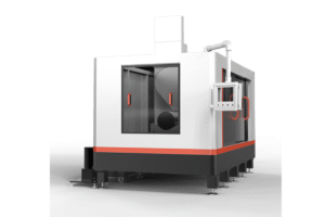
Wafer dicing methods continue to advance, especially in improving precision and performance due to ever-changing dynamics of smaller semiconductor devices. Dicing methods including laser technology that is precise and does not cause a lot of strain on the material, along with hybrid techniques, are bound to come into place.
Moreover, incorporation of automation and artificial intelligence may completely change how processes are controlled and how high yields are obtained. This will play an important role in the development of future generation electronics.
Future Perspectives of Silicon Wafer Cutting Technologies
Increased interests in high-volume manufacturing of integrated circuits and other micro devices will emerge adequately in the medium term. Research is already in progress to develop laser proton beam and very high-pressure water methods of slicing wafers as well as other materials like glass plates.
When less conventional loss-free segmented line methods are used, low-stress, free-standing, curved engravings are achieved. Such stress-free incisions are not feasible without requiring direct mechanical contact.
Emerging Technologies:
- Laser proton beam cutting for ultra-precise material removal
- Very high-pressure water jet methods for stress-free cutting
- Hybrid techniques combining multiple cutting approaches
- AI-driven process optimization and quality control
Conclusion and Recognized Methods
To maximize productivity in manufacturing of electronic equipment, it is preferable to use modern technological methods, including laser-based silicon wafer cutting technology or any hybrid method, for better control over operations and faster working proceedings.
The introduction of automation and artificial intelligence-based control loops into the process far improves performance through real-time supervision of activities and altering set processes as required. Recognized methods consist of performing equipment calibration timely, providing operators with training related to new technologies, and regulating accordingly the quality management process.
Key Takeaways Summary
Process Reliability
Improve through real-time monitoring and dynamic workflow adjustments
Equipment Calibration
Regular calibration achieves high accuracy and minimal operational mistakes
Operator Training
Regular training on new technological advances helps operators keep up with changes
Quality Management
Implementation contributes to uniformity of products and services rendered
Innovation Culture
Consistent innovation necessary for greater productivity and reduced material wastage
Machine Learning Integration
The use of real-time surveillance along with machine learning improves productive efficiency in manufacturing through predictive maintenance and production rationalization. Latest research shows that the use of machine learning in industry brings a reduction in unplanned downtimes of 50 percent and increases production output by 20-30 percent.
In addition, the technologies propose improved analytics tools to help manufacturers calculate potential process bottlenecks, automate quality checks, and optimize use of resources. This complementary function achieves process excellence and improved scaling of production processes.
Frequently Asked Questions
What is silicon wafer cutting?
Also called wafer dicing or die singulation, silicon wafer cutting is an essential step in the creation of microelectronic devices. The process results in accurate slicing of the silicon wafer with many embedded microcircuits, so that rectangular pieces called dies or chips can be removed and separated. These dies come in handy during production of various electronic components.
Why do we need wafer cutting?
A number of integrated circuits are produced at once in a single silicon wafer to optimize processes and enable savings. Wafer cutting is relevant to chop circuits into smaller pieces and isolate each one. This is necessary as dies have to be taken out from the remaining wafer so they can be placed in specific housing, mounted with connectors, and assembled into working electronic circuits.
What are the basic types of silicon wafer cutting?
The primary silicon wafer cutting techniques include:
- Diamond Blade Cutting: Traditional method using diamond-dotted saw at high speed along scribes on wafer surface. Can be used for many substances and wafer thicknesses.
- Laser Dicing: Laser beam concentrated on specific lanes to burn or vaporize material, offering excellent control with low material removal zones.
- Plasma Dicing: Avoids any induced cutting stresses, eliminates chipped edges, most suitable for processing very thin components and fragile structures.
What is “kerf” in silicon wafer cutting?
In silicon wafer cutting operations, “kerf” refers to the thickness of the area cut or ablated. Generally, narrower kerf comes best as more chips can be obtained from a single wafer, which ultimately enhances yield and reduces chip cost.
What are the problems in wafer cutting?
Several challenges within wafer cutting can affect yield and device function:
- Chipping and Cracking: Blade dicing may create small cracks or chipping leading to device failure
- Heat-Affected Zone (HAZ): Laser dicing may introduce high temperatures changing material properties
- Die Strength Weakening: Cutting creates structural weakness areas, lowering overall reliability
- Contamination: Dicing process produces silicon grit that can contaminate die surface if not cleaned properly
How do you select the appropriate cutting method?
Several criteria to consider when selecting cutting technique:
- Wafer Thickness: Thin wafers benefit from laser or plasma cutting
- Material Nature: Consider specific materials, films, and packages while selecting methods
- Die Dimensions and Interspace: Laser and plasma dicing used where minute spaces are required
- Device Sensitivity: Heat or stress-sensitive devices require non-contact dicing techniques
- Cost and Performance: Blade dicing is cost-effective for standard applications
How does stealth dicing work?
Stealth dicing is an improved silicon wafer cutting method that involves focusing the laser beam directly into the silicon wafer and not its topmost layer. It induces changes in the material layer, referred to as the stealth layer. The laser-treated wafer is then stretched over dicing tape and breaks along thin cleavage planes easily. This process eliminates production of surface residues and causes less thermal and mechanical damage, making it preferred for thin and delicate wafers.
Ready to Optimize Your Silicon Wafer Production?
With increasing culture of innovation and commitment to process improvement, manufacturers can be assured of high turnout rates, less material wastage, and continuous presence in the technocratic field of electronics.
Recommend reading: Gantry Diamond Wire Saw: Precision Cutting Technology
Related Posts
Trending Blogs

![Polysilicon Material: Properties, Grades & Uses [Guide]](https://wiresawcutter.com/wp-content/uploads/2026/08/polysilicon-material-featured-150x150.webp)