Get in touch with DONGHE Company
-
Phone: +86 181-1645-5490
-
Email: Sales18@DongheScience.com

Filter
Showing 25–29 of 29 results


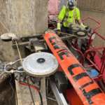
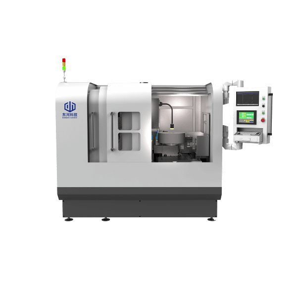
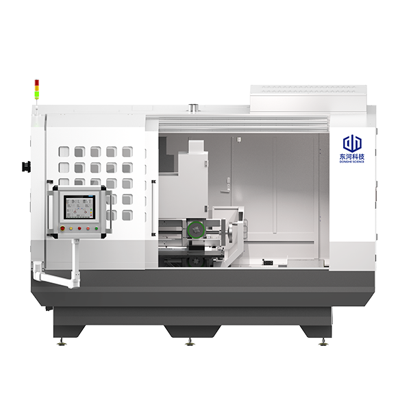
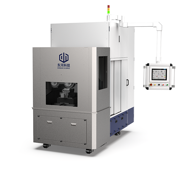
Endless Wire Saw Machine
Endless Wire Saw Machine for Precision Diamond Wire Cutting
Advanced endless diamond wire saw technology for cutting silicon, graphite, ceramics, and other hard materials. Achieve 60% less material waste with our continuous loop wire saw machines designed for semiconductor, solar, and laboratory applications.
0.35mm
Ultra-thin Kerf Width
80 m/s
Max Wire Speed
60%
Material Savings
What is an Endless Diamond Wire Saw?
On the other hand, an endless diamond wire saw, continuous wire saw, or loop cutting machine is high-precision cutting equipment established for cutting hard and brittle materials. Opposite to other cutting tools, it uses a closed diamond-coated wire running at an extremely high speed and continually moving in just one direction, usually around 60-80 meters per second.
This level of precision wire saw technology is a vast improvement for materials cutting in areas such as the semiconductor industry, photovoltaic manufacturing, optics manufacturing, and advanced ceramics. Traditional methods, such as wire cutting with slurry and band saw technology are far surpassed by the endless diamond wire saw.

High-speed unidirectional cutting (60-80 m/s)
Great surface finish (Ra 0.3-0.7 μm)
Minimal kerf loss (wire diameter 0.3-0.5mm)
Water-based coolant system (eco-friendly)
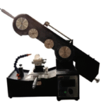
Key Components of an Endless Diamond Wire Saw
Critical to operating and maintaining an EDS machine is knowing which of its components are most important:
01
Diamond Wire Loop
Wire (with high tensile characteristics) coated and bonded with synthetic diamond beads (range typically 300-100 μm) used to cut into the materials.
02
Guide Wheel System
The guide rollers that help guide the wire while maintaining proper tension as cutting operations take place.
03
Tension Control
Maintains a constant tension on the wire at the range of 20-60 N.
04
Feed Mechanism
Operated by the user, completely controls how much the workpiece is fed to the wire.
05
Coolant System
It provides the coolant (water) to lubricate the cutting process and remove cutting debris on the diamond wire.
06
CNC Control System
The CNC controller, in combination with the motors, moves the cutting system in a precise, programmed manner for cutting complex shapes.
Types of Endless Diamond Wire Saw Machines
The modern endless wire saw and diamond wire saw cutting machines are available in various different types to meet different cutting requirements. The following will help you know all the types where you can choose one based on your application.
By Machine Structure

Vertical Wire Saw
In this case, the wire runs up-down while the workpiece to be cut feeds right to left. Best for cutting silicon ingot, laboratory samples, and common purposes because of its simplicity.

Horizontal Wire Saw
The wire runs crossing across. Most suitable for cutting rather free material like optical glass for slabs of large ceramics.

Gantry Wire Saw
These are big machines with the overhead wire system. For cutting big sapphire boules, very huge graphite blocks, or for on large-scale production.
Benchtop/Lab Wire Saw
Usually, a very compact machine serves well for research and development, quality control, and sample preparation. Found in universities and research labs.
By Cutting Capability
| Advantages | Disadvantages |
|---|---|
| High resolution | GPU dependency |
| Works with large masters | Best for classifying low number of unique outputs |
| Recursive scaling | Absence of reshuffling |
| Requires moderate training | Highly sensitive framework |
Free Precision Tools
Wire Saw Cutting Machine Calculator Tools
Calculate your potential savings and ROI for diamond wire saw cutting machine investment.
Input Parameters
pcs
mm
USD
Analysis Results
Real-time
Payback Period
14.4 months
Annual Savings
$50,000
42% cost reduction
3-Year ROI
285%
New Cost per Cut
$1.45
42% less
Efficiency Gain
+180%
5-Year Net Profit
$190,000
Cost Comparison (per cut)
Note: Calculations based on industry benchmarks. Contact us for a detailed custom analysis.
Material Parameters
g/cm³
mm
mm
cuts
pcs
mm
mm
Material Savings
Real-time
Annual Material Savings
$35,420
Saved per Cut
1.65 mm
Kerf Reduction
82.5%
Weight Saved
417 kg/yr
Extra Yield
+8.3%
More from same material
5-Year Savings
$177,100
Kerf Width Comparison
Key Insight: 82.5% less kerf = significant savings for high-value materials like sapphire and SiC.
Ready to Optimize Your Wire Saw Cutting Process?
Get a personalized ROI analysis for your wire saw cutting machine investment.
Common Cutting Challenges Solved by Precision Wire Saw Machine
Cutting through hard and brittle materials the manufacturers' way is entirely fraught with problems which they have to face on the other side of the chasm, i.e., traditional cutting methods. Here are some of the core issues that we hear from our customers before they move on to diamond wire saw technology:
Critical Industry Challenges
Material Wastage at Exorbitant Rates (High Kerf Loss)
ID saws and band saws, which are the traditional ones, give kerf widths of 0.8-1.5mm, which is as much as 2-3 times more than the required material being wasted. The wastage is particularly there in the case of expensive substrates like silicon carbide (SiC) or sapphire whose prices range from $50 to $500+ per wafer, and as a result, this loss greatly affects production costs and yield.
Surface Quality is Poor and Subsurface Damage is High
The use of aggressive cutting has resulted in the creation of rough 1.5μm surfaces and layers beneath the surface that have been damaged up to 50μm deep in some instances. This has necessitated lapping and polishing which has indeed consumed time and money while also creating the risk of further material loss.
Edge Chipping/Breakage
Cutting brittle materials such as ceramics, glass, and thin wafers often leads to edge chipping, micro-cracks, and workpiece breakage. Yield losses of 5-15% are usual with the conventional methods.
Challenge to Cut Non-Conductive Materials
Graphite, glass, and advanced ceramics are among the materials that cannot undergo EDM wire cutting. Traditional mechanical methods generally yield poor results.
Slow Cutting Speed & Low Throughput
Reciprocating wire saws and slurry-based systems are physically limited to lower speeds, which restricts productivity. Long cycle times not only reduce output but also add to the per-unit costs.
Complex Operation & Maintenance
The use of some cutting systems requires a highly trained operator, regular adjustments, and elaborate maintenance procedures, all of which ends up increasing operational costs and downtime.
Doubt in Equipment Selection
There being plenty of cutting technologies available, the decision about which equipment to use for specific materials and applications can be very difficult so it may also lead to wrong investments that are costly.
Precision Wire Saw Machine Solutions
Eliminate 50%+ of the kerf loss by cutting with ultra-thin wire.
We use diamond wire loops with the smallest diameter being 0.30mm in our endless wire saw machines and this leads to the production of kerf widths just between 0.35-0.45mm. Compared to ID saws (0.8-1.2mm kerf), you reclaim 30-50% more material per workpiece. For a 200mm SiC ingot, this can amount to an extra 10-15 wafers per ingot.
Get Surface Quality that is Superior (Ra)
Cutting done in one direction only eliminates vibrations and yields very smooth surfaces. The parameters that we optimized result in surface roughness Ra 0.3-0.8μm for most materials with the subsurface damage being not more than 5μm, this quite often leads to less or no lapping and polishing time being reduced by 50%.
Eliminate Edge Chipping with Soft Cutting Action
The flexible diamond wire loop during cutting exerts a minimal lateral force. In conjunction with the feed rates and tension control that have been optimized, our machines cut brittle materials, for instance, thin silicon wafers and ceramics, without edge chipping thus increasing yield to 98%+ even for fragile workpieces.
Cut Any Hard Material – It Doesn't Matter if it is Conductive or Not
Diamond wire cutting is purely mechanical and works on any material that is softer than diamond. From conductive metals to insulating graphite, optical glass, and advanced ceramics – one machine can handle all these and more. Perfect for the facility that processes multiple material types.
Increase Output with High-Speed Continuous Cutting
Running at speeds of up to 60 m/s (3-4x faster than reciprocating systems) and combined with continuous loop operation results in significantly shorter cycle times. Our customers' productivity increases of 40-100% over their previous cutting equipment are reported.
Simplified Operation & Lower Maintenance Costs
The endless wire saw machines we offer come with user-friendly controls, quick replacement of the wire loop (in less than 10 minutes), and require minimal maintenance. Operators can be trained in just a few hours as opposed to weeks thereby reducing operational overhead.
Expert Application Support and Custom Solutions
Our engineering team of diamond wire cutting professionals with over 15 years of experience provides free cutting tests, parameter optimization, and customized solutions tailored to your specific material and production requirements.
Endless Wire Saw Machine Industrial Applications & Materials
Our endless wire saw machine which are endless by nature cater to various industries asking for the cutting of hard and brittle materials with precision. Following are the major applications and the materials that we cut:

Semiconductor Manufacturing
Cropping of silicon ingot, wafer sampling, SiC & GaN processing

Photovoltaic Industry
Cutting of mono/poly silicon, production of solar cells
LED & Optoelectronics
Cutting of sapphire substrate, processing of LED wafer

Optical Components
Glass for optical, quartz, materials for lens

Advanced Ceramics
Alumina, zirconia, SiC, Si3N4 ceramics

Magnetic Materials
NdFeB, ferrite, and rare-earth magnets
Endless Wire Saw Machine vs. Traditional Cutting Technology
Endless Diamond Wire Saw technology vs. traditional cutting methods. See performance comparisons across multiple metrics.
Cutting Speed
Linear velocity (m/s)
3-4x Faster
Kerf Loss / Material Waste
Cut width (mm)
85% Less
Surface Roughness (Ra)
Lower is better (μm)
Superior Finish
Operating Cost Index
Relative cost per cut
30% Savings
Endless Wire Saw
Band Saw
Slurry Wire Saw
ID Saw
Detailed Specifications Comparison
| Specification | Endless Diamond Wire Saw | Diamond Band Saw | Slurry Wire Saw | ID Saw |
| Cutting Speed | 60 - 80 m/s | 10 - 20 m/s | 5 - 15 m/s | 20 - 30 m/s |
| Kerf Width | 0.3 - 0.5 mm | 1.5 - 3.0 mm | 0.15 - 0.25 mm | 0.8 - 1.2 mm |
| Surface Ra | 0.3 - 0.7 μm | 1.5 - 5.0 μm | 0.3 - 0.5 μm | 0.8 - 2.0 μm |
| TTV Control | ± 5 - 10 μm | ± 20 - 50 μm | ± 3 - 8 μm | ± 10 - 20 μm |
| Throughput | High | Medium | Low | Medium |
| Environmental | Water-based | Water/Oil | Slurry waste | Water/Oil |
| Maintenance | Low | Medium | High (slurry) | Medium |
| Operating Cost | Low-Medium | Low | High | Medium |
How to Choose the Right Endless Wire Saw Machine
The choice of a diamond wire cutting machine has to take into account various application requirements that are specific to your case. To get a good choice, follow this selection guide:
1
Workpiece Dimensions
Your maximum workpiece size is the most important factor. Check that the cutting capacity of the machine is larger than that of your biggest workpiece, with a safety margin:
Benchtop:
Samples up to 100 mm
Standard industrial:
100-400 mm workpieces
Large format:
400 mm+ materials
2
Material Hardness & Properties
Different wire specifications and cutting parameters depend on the materials:
Silicon, SiC, Sapphire:
Electroplated wire with fine grit (40-80μm) is used
Optical glass, Quartz:
Medium grit (60-100μm), water cooling
Ceramics:
Brilliance and brittleness are the factors to play with, lower feed rates are the way to go
Graphite:
Grit can be coarser and dry cutting can be done
3
Required Accuracy & Surface Quality
Application
Required Surface Finish
Semiconductor wafer prep
Ra < 0.5μm, no SSD
Optical components
Ra < 0.3μm is often the case
Structural ceramics
Ra 0.5-1.0μm is ok
Graphite processing
Ra 1.0-2.0μm is often enough
4
Production Volume
R&D/Low volume:
Manual or semi-automatic machines
Medium production:
Programmable with basic automation
High volume:
Fully automated with loader/unloader integration
Important
Don't oversize your machine unnecessarily. A machine that is too large may have less accuracy for small workpieces. The machine capacity should be matched to your typical (not maximum) workpiece size, allowing for a reasonable headroom for occasional larger pieces.
Why Choose Us Our Endless Wire Saw Machines
1
Maximum Material Yield
The most substantial material loss is reduced by 60-70%, when compared to band saws, which means that in a cropping operation of a 6" SiC ingot, the yield is increased by 2+ wafers, and this will eventually cut the cost significantly.
2
Superior Surface Quality
The ultra-fast uninterrupted cutting process gives rise to mirror-like surfaces (Ra
3
Faster Cutting Speeds
Wire operating at speeds of 80 m/s—3 times quicker than reciprocating systems—provides more output without compromising on quality of the cut. Efficiently meet the production requirements.
4
Reduced Operating Costs
Shorter wire loops (2-10m vs 20-40m) bring down the cost of consumables. The uncomplicated mechanical designs result in less wear-and-tear and longer service intervals.
5
Versatile Material Handling
With the same machine, perform cutting of silicon, graphite, ceramics, glass, etc. Easy switching of parameters allows quick and efficient processing of many different materials.
6
Expert Application Support
Your productivity will be maximized by our engineering team providing cutting parameter optimization, operator training, and technical support throughout.
Endless Wire Saw Machine Case Studies
The Challenge
During the peak shifts in demand for electric vehicles and renewable energy systems, the client experienced a critical SiC (Silicon Carbide) wafer production line bottleneck. Under both the necessary quality and efficiency parameters, the pre-existing ID (Inner Diameter) saw system had a considerable performance deficit:
- Excessive Kerf Loss: The ID saw cutting width created a 0.8mm kerf, resulting in lost materials that were worth over $3,000 per 6-inch SiC ingot.
- Surface Damage: Depths of subsurface damage exceeded 15µm which necessitated excessive post-processing.
- Low Throughput: Over 45 hours were required per 6-inch SiC ingot to fully process it into wafers.
- Blade Changes: Production disruptions were caused by ID blade replacements which needed to be made every 200 cuts.
The client's engineering team made a request for a diamond wire saw for semiconductor applications which could effectively increase the surface quality while simultaneously decreasing the material waste.
Our Solution
Our application engineering team prepared a proposal consisting of the client's needs as well as the SV-360H Endless Diamond Wire Saw Machine configured for cutting SiC wafers:
Diamond Wire:0.35mm loop electroplated with diamond (40/50 mesh grit)
Wire Speed:Optimized at 18-22 m/s to target SiC hardness
Feed Rate:0.5mm/min (with a progressive feed algorithm)
Coolant System:Dual-flow water cooling with 15°C control
Tension Control:±0.5N automatic wire tension control
Week 1-2Installation of the machine and assessment on site
Week 3-4Testing of optimization parameters with test ingots
Week 5-6Documentation of processes and training of operators
Week 7-8Quality certification and validation of production
Results Achieved
| KPI | Before (ID Saw) | After (SV-360H) | Improvement |
|---|---|---|---|
| Kerf Loss | 0.80mm | 0.38mm | Reduced by 42% |
| Surface Roughness (Ra) | 0.8μm | 0.3μm | Improved by 62% |
| Subsurface Damage | >15μm | <5μm | Reduced by 67% |
| Processing Time (6" ingot) | 45 hours | 28 hours | Faster by 38% |
| Wafers per Ingot | 85 wafers | 112 wafers | Increased yield by 32% |
"Replacing our SiC production line with the endless diamond wire saw system was a remarkable improvement! This has resulted in a 42% reduction in kerf loss, resulting in annual savings exceeding $180,000 on raw material costs. Most importantly, the enhanced surface quality minimizes downstream polishing time by 40%, significantly improving our time-to-market for new power semiconductor products."
Key Takeaways
- Endless wire saw technology is perfectly suitable for hard shatterable compound semiconductors such as SiC and GaN
- Maximizing productivity is dependent on correct wire choice and parameter optimization
- Material cost savings can yield a return on investment in as little as 6 to 8 months when using costly substrates
- Reduced subsurface damage greatly reduces subsequent processing needs
The Challenge
With the world's current focus on renewable energy, our client, a leading photovoltaic silicon producer, needed to quickly increase the capacity of his company's monocrystalline wafer while remaining cost competitive:
- Capacity limitation: Current multi-wire slurry saws do not suffice to achieve the 40% increase in output target
- Waste of silicon: Slurry-based cutting resulted in 70μm of kerf loss per cut, which totalled to over 15% silicon waste of the total output
- Silicone waste: The waste generated from cutting sawern a new environmental challenge with additional cost for environmental compliance
- Wafer Thickness Demand: In order to achieve wafer thickness of 150μm, the demand is for equipment with increased precision
- Cost Pressure: In order to keep cutting sufficiently, it is necessary to keep reduce the costs incurred over the cutting of each wafer by 20%, at a minimum
Our Solution
For high volume cutting of silicon wafers, we proposed an upgrade of the entire production line for our SVO-500 Series Industrial Endless Wire Saw systems.
Wire Type:0.30 mm electroplated endless diamond wire loop
Cutting Capacity:silicon ingots of 210 mm in diameter
Wire Speed:25-35 m/s with speed control that is adjustable
Automation:Fully automated with integrated robotics for loading and unloading
Monitoring:TTV (Total Thickness Variation) monitoring system in real time
Coolant:Closed loop with water recycling and filtration (95% of water is reused)
Phase 1Installation of 1 unit for the pilot process validation (4 weeks)
Phase 2Certification for production optimization and operator (3 weeks)
Phase 3MES integration for the deployment of the remaining 2 units (6 weeks)
Phase 4Production support with remote monitoring for 24/7 ramp up (ongoing)
Results Achieved
| Metric | Before (Multi-Wire Slurry) | After (SVO-500) | Improvement |
|---|---|---|---|
| Kerf Loss | 0.18 mm | 0.12 mm | 33% reduction |
| Wafers per Ingot (182 mm) | 5,200 wafers | 7,020 wafers | 35% more yield |
| TTV (Total Thickness Variation) | ± 15 μm | ± 8 μm | 47% improvement |
| Cutting Cost per Wafer | $0.042 | $0.028 | 33% cost reduction |
| Water Utilization | 100% | 5% (95% Recycled) | 95% Reduction |
| Daily Output (3 Units) | 45,000 Wafers | 72,000 Wafers | 60% Increase |
"Switching to the Endless Diamond Wire Saw technology was key for our expansion strategy. The 35% kerf loss improvement yield translated to millions of savings annually. However, the slurry waste elimination and 95% water consumption reduction was the environmental benefit that helped us meet our sustainability certifications ahead of schedule."
Key Takeaways
- Endless diamond wire technology allows thinner wafer production with enhanced TTV control
- The reduction of slurry elimination means lower operational costs and less environmental compliance issues
- Automated systems with MES integration enables 24/7 high-volume production
- Closed-loop coolant systems lower water usage and reduce operational costs
The Challenge
The customer provides high-purity alumina ceramic substrates for automotive power modules for electric vehicles. The automotive power module customer's quality demands are among the most stringent in the industry:
- Edge quality: Any visible edge damage results in rejection, chipping tolerance is zero
- Dimensional precision: Substrate dimensions have a tolerance of ±0.02mm
- Surface integrity: Micro-cracks are a No Go. They must pass fluorescent penetrant inspection
- High reject rate: Designed diamond blade dicing saw produced edge chipping at a rate of 8-12%
- Throughput pressure: EV market growth required a 50% capacity increase in less than 6 months
The client needed a ceramic cutting machine, able to deliver automotive-grade quality at much higher volumes.
Our Solution
We have constructed a procedure using our SV-280P Precision Endless Diamond Wire Saw, designed for brittle ceramic materials.
Diamond Wire:D 0.28mm resin bonded diamond wire (ceramic optimized)
Cutting Mode:Ductile-mode cutting to reduce brittle fracture
Wire Speed:8-12 m/s. Low-speed mode
Feed Control:Constant-force feed. 0.1N sensitivity
Fixturing:Custom vacuum chuck with stress-free substrate
Coolant:For high purity processed, deionized water with free running pH
Step 1Material Analysis: studied both 96% & 99.6% alumina's cutting behavior
Step 2Parameter Development: optimized speed/feed for each alumina type
Step 3Edge Quality Validation: chip-free edges, confirmed via SEM 500x
Step 4Process Certification: IATF 16949 Cpk > 1.67
Results Realized
| Metric | Before (Blade Dicing) | After (SV-280P) | Improvement |
|---|---|---|---|
| Edge Chipping Rate | 8-12% | <0.3% | 97% decrease |
| First-Pass Yield | 88% | 99.7% | Nearly zero defect |
| Dimensional Accuracy | ±0.05mm | ±0.015mm | 70% increase |
| Surface Roughness (Ra) | 1.2μm | 0.4μm | 67% increase |
| Cutting Speed | 2 substrates/min | 3.5 substrates/min | 75% increase |
| Tool Cost per Substrate | $0.15 | $0.06 | 60% decrease |
"The SV-280P exceeded our expectations for precision ceramic cutting. Achieving 99.7% first-pass yield means we've virtually eliminated rework and customer quality complaints. In particular, our automotive OEM clients have praised us for our improved edge quality, which has strengthened our position as their preferred substrate supplier."
Key Takeaways
- The edge chipping in ceramics is removed by resin-bonded diamond wire with ductile-mode parameters
- It is important to use constant-force feed control when processing brittle materials
- Good fixturing design eliminates stress-induced micro-cracks
- Automotive-grade quality certification (IATF 16949) is possible with wire saw technology
The Challenge
As a materials research leader, the laboratory receives hundreds of different samples monthly for microstructural analysis, such as:
- Composite materials: Carbon fiber reinforced polymers, ceramic matrix composites
- Electronic components: Multi-layer PCBs, semiconductor packages, battery cells
- Metallurgical samples: Superalloys, titanium alloys, additive manufactured parts
- Geological specimens: Rock cores, mineral samples, fossils
Their preparation techniques were limited in the following ways:
- Heat damage: Excessive sample microstructure alteration due to the use of abrasive cut-off wheels
- Delamination: The multi-layer samples often delaminated during cutting
- Variety of equipment: Different materials needed different cutting systems, adding to lab complexity
- Slow Turnaround: Difficult samples took 2-3 days to complete proper sectioning
The lab needed a versatile laboratory wire saw to accommodate their varied material portfolio.
Our Solution
We have delivered one SV-150L Laboratory Endless Wire Saw, customized for the flexibility and precision found in research environments:
Small Design:Benchtop (600 x 500 x 450mm) for additional compact standard lab spaces
Multi-Wire System:0.20-0.50mm diamond wires with quick-change
Wire Library:For a range of different materials, 6 types of wire are included
Variable Speed:1-25 m/s tailored for specific materials
Low-Force Mode:For sensitive samples, cutting force is adjustable down to 0.05N
Cutting Window:For observing the cutting process, the chamber is LED-illuminated
Software:100+ different cutting programs stored by recipe
Day 1System calibration, and installation
Day 2-3Training with sample materials
Week 2-4Priority materials collaborative parameter setting
OngoingSupport and parameter adjustment remotely
Results Achieved
| Metric | Before | After (SV-150L) | Improvement |
|---|---|---|---|
| Sample Turnaround Time | 2-3 days | 2-4 hours | 90% faster |
| Thermal Damage | Frequent | None detected | Eliminated |
| Composite Delamination Rate | 25% | <2% | 92% reduction |
| Materials Processable | Limited selection | 50+ material types | Universal capability |
| Equipment Footprint | 3 different systems | 1 compact unit | 67% space reduction |
| Sample Quality for SEM/TEM | 60% acceptable | 95% acceptable | 58% improvement |
"The SV-150L has become the workhorse of our sample preparation lab. Previously, three cutting systems and a day-long process would now be done in a matter of hours with one machine. Even our graduate students can prepare publication-quality cross-sections consistently, thanks to the ability to store recipes for specific materials. It's transformed our research throughput."
Key Takeaways
- Endless wire saws provide cold-cutting, crucial to preserving microstructures
- Micro wire compatibility eliminates multiple cutting system needs
- Recipe storage ensures reproducible results across different operators
- Low-force cutting prevents delamination in layered/composite materials
Endless Wire Saw Machine FAQs
How does a wire saw with diamond power work continuously, and how does it differ from the diamond wire saw?
A diamond wire saw is more like a cutting machine using a closed-loop diamond wire or a flexible cutting wire with inserted diamond abrasives; it uses the two together to give a precise cut at hard, brittle materials. The arm with diamond-coated wire returns to cut around the sample stage after having been heated and cooled with coolant. The frictional heat from the cutting process will be conducted through the diamond abrasive to the sample stage. The roller's drive and holding unit further finalize the movement of the diamond-coated wire. Therefore, it is a strong generator of the cutting process. These kinds of wire saws find their application in materials as silicon, quartz, sapphire, optical glass, ceramics, and graphite.
Why does there exist a need to use diamond wire cutting machines for cutting processes engaged with hard and brittle materials?
Diamond wire cuting mcahines were intrduced to perform percision wire ctuing and high-speed elsless loop operations for carving heard material like silicon carbide, alumina, and sapphire. The longend bucke coated wire of superior quality and diamond-cutting method provide better quality cutting, less damage to the layers beneath the surface of the cut material, fast cutting compared with conventional saw blade cutting or blade cuttings. Manufacturers design these solutions to meet cutting requirements for cutting process of the semiconductor, aerospace, and optician glass industries.
Can diamond wire saw be used for graphite cut and silicon wafer slicing at the same time?
Sure. Wire saw cutting is effective in graphite cut and silicon wafer slice applications. The diamond wire machines and loop type diamond wires can cut graphite or silicon with a good control of slice thickness. Features such as a digital micrometer and two angularly adjustable or a two angularly adjustable sample stage improve accuracy for thin slicing required in the semiconductor and crystal processing.
Materials to be cut by diamond wire include optical glass and ceramics.
Diamond wire cutting can be successful in a wide variety of materials that are hard and brittle: optical glass, ceramics, quartz, sapphire, GaAs and YVO4, which are semiconductor materials, and gemstones. The extremity of diamonds enables these materials to be cut efficiently and with minimal chipping. Softer sets of material, such as alloy or epoxy with a less-hard abrasive, can also be cut, but usually need a modified cutting speed, coolant, or an appropriate diamond grit for optimizing the cutting quality and the use-history of the cutting wire.
What role does the cutting speed, diameter, and loop type play in determining cutting quality and efficiency?
The fastest failing, by a long shot, about half the samples measured in each case had a very different design from the other half. Speed, wire diameter, and looping type are key controllers required for fast cutting to get good results. The circuit surface runs at high speeds, which enhances throughput, although wire diameter and diamond grit must reach a balancing point to prevent significant wear. Thin wire diameters produce a fine kerf and offer higher wire cutting accuracy whereas thick diameters are conducive to high wire cutting robustness. Loop type diamond wire and spooler driving mechanisms lead to the impulsive promotion on a stable and constant cutting speed that greatly influences the types of material to be cut, cut quality, and also other factors.
Any accessory and control improvements that enable better precision on diamond wire machines (such as micrometer and sample stage)?
Precision cutting is advanced by accessories such as movable sample stage with twin angle alignment, digital micrometer, double antenna control, wire loop tension monitors, and coolant life enhancing systems. All these contribute to the working process, enabling correct gemstone cutting, optical glass cutting, and sliced semiconductor. Certified endless wire saw models for precision (CE, ISO) usually come with these components, having a Q/QC etc. (and other quality control options), along with possible NTRL certification via mlti for work place safety and assurance.
What is the impact of coolant and coverage on long-term maintenance and cutting performance?
Maintaining the cutting interface temperature, rejecting debris, and giving the diamond wire the longest durability are placed in necessary roles. Proper coolant selection and flow can inhibit the heat ausmol. A regular maintenance regime elaborates on replacing spool drives, checking wire loops, ensuring tension, and checking filtration for operational quality and to avoid unnecessary disruptions. Further recommendations could be found from the manufacturers on maintenance intervals and required consumables to match a particular cutting environment.
Are VimFun's diamond wired saws suitable for industrial use?
VimFun saws, cutting socks, and some other established manufacturers are more likely to offer a variety of wire machines options, ranging from a basic wire saw to a precision endless wire saw with advanced control and calibration. It is likely that cutting eloquent speed, wire cutting accuracy, sample tray design, certification (CE, ISO), and materials that may include silicon, graphite, sapphire, etc., will all have to be compared between models. Accredited manufacturers offer documentation on cutting technologies, cutting procedures, and spare parts in order to ensure that there are safe and effective cutting solutions.
What safety, certification, and application considerations are important when selecting a cutting machine?
The act of using wire cutting machinery in industries brings alarm for safety and certification (CE, ISO, and optionally NRTL organized by mti). The evaluation of the guarding of the machine, emergency stop, containment of coolant, and training support should be part of the discussion. Consider application requirements (semiconductor, optical glass, ceramics), proposed slice thickness, cutting speed, and production volumes. For specialized work like gemstone cutting or multi-wire cutting, consult the manufacturers to ascertain diamond wire cutting machine requirements and fine-tune the cutting solutions for fast, high-precision wire cutting applications.