Get in touch with DONGHE Company
-
Phone: +86 181-1645-5490
-
Email: Sales18@DongheScience.com

How Computer Chips Are Made: From Silicon Wafer to Final Chip
Quick Specs
| Starting material | High-purity silicon crystal sliced into wafers |
|---|---|
| Core wafer step | Ingot slicing, lapping, polishing, cleaning, and inspection |
| Patterning method | Photolithography; EUV for selected advanced nodes |
| Repeated fab cycle | Deposit or grow film, coat resist, expose, develop, etch, dope, clean, inspect |
| Back-end steps | Wafer probe, dicing, packaging, burn-in or final test |
| Buyer bridge | Wafer cutting affects kerf loss, TTV, surface damage, breakage risk, and later yield work |
Microchips are made in fabrication facilities, but the shorthand can hide the chain. In beginner explanations, sand is melted and refined into pure silicon; after crystal growth, the ingot is sliced into thin wafers. During chip fabrication, materials are added by methods such as chemical vapor deposition and physical vapor deposition. A layer of silicon dioxide may act as an insulator before a process known as photolithography and a process called doping set the pattern and conductivity.
Silicon chips are made of silicon, and most mainstream microelectronic devices are made from silicon wafers, yet chip design decides whether the result becomes analog chips, digital chips, application-specific integrated chips, memory, or processor devices. The type of chip sets electrical connections, package choice, and how the final device will process data for computer processing. Because features can be nanometers in size while wafers are measured in millimeter-scale thickness, microchip manufacturing needs both chip technology and precision material handling to make chips at scale. Later, the wafer is cut into die.
In the semiconductor industry, microchips made for phones, vehicles, servers, and control boards are a set of electronic circuits formed through the chip industry supply chain. Extreme ultraviolet lithography works on incredibly small features, while dopants change the properties of the silicon before the wafer becomes a finished device.
How Are Computer Chips Made? 9-Stage Process At A Glance

Use the Wafer-to-Chip 9-Gate Map as the working mental model. Each gate turns raw material into something closer to a working electronic circuit. It also shows where process errors start to cost money.
| Gate | Main work | Defect risk | Control point | Buyer or engineer question |
|---|---|---|---|---|
| 1 | Purify silicon | Wrong impurity level | Resistivity and crystal quality | Which grade is required? |
| 2 | Grow ingot | Crystal defect | Orientation and dopant profile | What wafer diameter and orientation? |
| 3 | Slice wafer | Kerf loss, TTV, subsurface damage | Wire speed, wire diameter, tension | Can the saw hold flatness? |
| 4 | Polish and clean | Particles, roughness, stains | Surface roughness and cleanliness | What inspection follows slicing? |
| 5 | Build films | Non-uniform layers | Film thickness and stress | Is the wafer ready for repeat cycles? |
| 6 | Print patterns | Alignment or exposure error | Overlay and linewidth | Which lithography step sets the limit? |
| 7 | Etch and dope | Wrong geometry or conductivity | Etch profile and ion dose | Can later layers still align? |
| 8 | Test and dice | Bad die, chipped edge | Wafer probe and dicing quality | How are weak die handled? |
| 9 | Package and final test | Thermal or connection failure | Package reliability and final test | What device class is being shipped? |
Computer chips are not a single material operation. They come from a sequence of material science, optics, chemistry, electrical testing, and packaging choices. That is why a short disruption in one step can slow the whole line.
Silicon First: Why Computer Chips Start As Wafers

Silicon matters because its electrical conductivity can be tuned. NIST describes materials such as silicon as the base for integrated circuits because they make complex chips possible for computing, communications, health, transport, and other electronics.
In practice, chip manufacturing starts with a single-crystal silicon ingot. Manufacturers shape the ingot and slice it into thin circular wafers. BYU Cleanroom defines a wafer as a thin circular slice of single-crystal semiconductor material cut from an ingot and used for semiconductor devices and integrated circuits.
Standard silicon wafer diameters range from small research wafers to 300 mm production wafers. Larger wafers can carry more die per process run, but they also raise the bar for flatness, bow, warp, and Total Thickness Variation. Poor slicing quality creates extra work before the first circuit layer is built.
For readers comparing equipment, DONGHE’s silicon wafer cutting wire saw page is the relevant bridge from chip explanation to wafer preparation. Fabs may get the spotlight, but the wafer enters that fab with a history: ingot growth, slicing, surface work, cleaning, and inspection.
Wafer Fabrication: The Repeat Cycle That Builds Chip Layers

Once a polished silicon wafer enters wafer fabrication, the work becomes repetitive by design. No fab draws the whole electronic circuit in one pass. Instead, it builds a stack of thin films, patterned regions, insulators, doped zones, and metal paths through repeated cycles.
| Cycle step | What happens | What can go wrong |
|---|---|---|
| Grow or deposit | Add silicon dioxide, metal, dielectric, or other films | Thickness drift, stress, contamination |
| Coat resist | Apply light-sensitive photoresist | Coating voids, particles, poor adhesion |
| Expose and develop | Transfer mask pattern to the wafer | Overlay error, linewidth drift |
| Etch | Remove exposed material | Sidewall damage, residue, over-etch |
| Dope | Add controlled impurities to change conductivity | Wrong dose or depth |
| Clean and inspect | Remove residues and measure results | Particles remain; bad wafers keep moving |
NIST describes semiconductor facilities with instruments that lay down thin layers on silicon wafers, transfer patterns, and remove material to make custom chips. That short description is the heart of wafer fabrication.
Photolithography And EUV: How Tiny Circuit Patterns Are Printed

Photolithography transfers a circuit design to the wafer. Engineers coat the wafer with photoresist, expose it through a mask, develop the image, and then send it onward for etching or other steps. Engineers may repeat the patterning cycle again and again until transistors and interconnects form a multi-layer electronic circuit.
How are computer chips made step by step?
Step by step, computer chips are made by purifying silicon, growing a crystal ingot, slicing that ingot into wafers, polishing and cleaning each wafer, depositing films, printing circuit patterns with photolithography, etching selected material away, doping regions to control electrical current, forming interconnects, testing the wafer, dicing it into individual chips, packaging those die, and testing the finished device. Some chips use mature process nodes with deep ultraviolet tools; selected advanced chips use EUV lithography for the tightest patterning steps.
| Lithography type | Light wavelength | Why it matters | Hard part |
|---|---|---|---|
| Deep UV | 193 nm | Used for many high-volume patterning layers | Multi-patterning and overlay control |
| EUV | 13.5 nm | Helps print smaller features in fewer patterning moves | Vacuum path, source power, mirrors, resist, contamination |
NIST’s EUV work gives the engineering reality behind the shorthand. EUV is not just “shorter light.” Air absorbs it, mirrors can lose reflectivity, materials outgas, and carbon contamination can form under EUV photons.
“That’s going to be a big change.”
Etching, Doping, And Interconnects: How The Circuit Starts To Work

After exposure and development, etching removes material in selected areas. Wet etching uses chemistry. Dry etching uses plasma. Either way, the goal is controlled removal, not rough cutting. Good etching preserves the pattern and prepares the next layer.
Doping changes silicon’s electrical properties. BYU Cleanroom defines a dopant as an element intentionally introduced into a semiconductor to establish p-type or n-type conductivity, with boron, phosphorus, arsenic, and antimony among silicon examples. Those small impurity additions are why a region can act as part of a transistor rather than as plain silicon.
Engineering Note: Contamination Is Not A Small Detail
NIST notes that shrinking chips become more sensitive to contamination, and its EUV work found mirror contamination behavior that was not linear with pressure. That matters because a chip line is built around measurement. Cleaner, flatter, lower-damage wafers do not guarantee yield, but they reduce the number of avoidable problems before patterning even begins.
Interconnect formation then links transistors into circuits. Metal lines and insulating layers turn isolated device structures into a logic chip, memory chip, microprocessor, sensor, or power device. This microscopic circuitry can include transistor regions, resistor structures, and other building blocks wired into a stacked city at nanometer scale.
Test, Dice, Package: When The Wafer Becomes Individual Chips

A wafer does not become a tray of finished chips the moment patterning ends. First, the wafer is probed. Electrical tests identify which die meet the design target, which die can be sold at a lower grade, and which die must be discarded.
Dicing cuts the wafer into individual chips. BYU Cleanroom defines dicing as cutting a semiconductor wafer into individual chips, each containing a complete semiconductor device. After that, each die is attached to a package, connected to external contacts, protected from handling and environment, and tested again.
| Area | Main output | Reader takeaway |
|---|---|---|
| Front end | Patterned wafer with working die | Most transistor formation happens here |
| Probe | Known-good and failed die map | Yield is measured before dicing |
| Dicing | Individual die | Mechanical quality still matters |
| Packaging | Protected chip ready for board use | Thermal, power, and signal paths are finished here |
This is why “perfect chips” is the wrong mental model. Fabs expect variation. They test, sort, repair where possible, and package only devices that meet the target for a given product class.
Why Advanced Semiconductor Computer Chips Are Hard To Make At Scale

The difficulty is not one mystery machine. It is many narrow control windows stacked together: crystal growth, wafer flatness, particle control, photoresist behavior, lithography source stability, etch shape, dopant dose, metal fill, inspection, packaging, water supply, and tool uptime.
How many gallons of water does it take to make a microchip?
There is no honest single number for one microchip without knowing the wafer size, die size, process node, layer count, yield, water reuse, and fab design. Safer answers work at wafer or fab scale. WEF/Ceres reported in 2024 that an average chip manufacturing facility can use about 10 million gallons of ultrapure water per day, while older CWR analysis discussed a 30 cm wafer example requiring about 2,200 gallons of water. Treat per-chip water estimates as scenario math, not a fixed spec.
Why can’t the US produce chips like Taiwan?
U.S. fabs can produce chips, but the most advanced foundry capacity has been concentrated in Taiwan and South Korea for years. NIST cites SIA data that the U.S. had 12 percent of global semiconductor manufacturing capacity on its semiconductors page, while pointing to measurement science, standards, materials, instrumentation, testing, and manufacturing capability as areas needed for next-generation microelectronics. Rebuilding capacity takes fabs, suppliers, trained workers, process recipes, yield learning, and demand commitments.
Advanced chips are hard because each layer carries previous errors forward. Even if a wafer with surface damage enters a process, the cost of finding that weakness rises later. Tiny lithography drift may not show up until electrical test. Water outages can stop a fab line. Packaging choices can limit heat removal even when the die itself works.
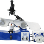
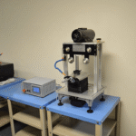
Where Diamond Wire Sawing Fits In The Chip Supply Chain

Diamond wire sawing belongs near the start of the silicon wafer story. It is not the same as photolithography, etching, or packaging. Its job is to turn a hard, brittle ingot or material block into wafers or samples with controlled kerf, thickness, surface quality, and breakage risk.
DONGHE reports process ranges on its silicon wafer cutting page including 10-25 m/s wire speed, 60-120 um wire diameter, 20-40 N wire tension, feed rate of 0.3-1.0 mm/min, TTV under 10 um, Ra 0.3-0.6 um, and kerf loss of 60-120 um. Those are page-reported ranges, not universal specs for every fab. They are useful screening questions for buyers comparing a silicon wafer cutting wire saw with a SiC wafer cutting saw, sapphire cutting wire saw, or ingot cropping wire saw.
| Application | Main risk | Cutting question | Procurement signal |
|---|---|---|---|
| Solar silicon wafer | Kerf loss and throughput | What wire diameter and speed stay stable? | Throughput plus material-loss data |
| IC silicon wafer | TTV and subsurface damage | How is flatness checked after slicing? | Inspection and process-control records |
| SiC or GaN wafer | Tool wear and edge chipping | Which wire bond and grit are used? | Hard-material cut history |
| R&D sample | Small-lot loss | Can fixtures handle custom shapes? | Repeatable setup notes |
Buyers who need low-volume tests can also compare laboratory diamond wire saw options with precision diamond wire saw systems. For brittle substrates, DONGHE’s hard and brittle material cutting wire saw category is the wider application hub.
Wafer-Cutting Readiness Matrix For A Trial Run
A supplier conversation works better when the buyer brings a decision matrix, not only a material name. The matrix below is a pre-trial checklist for selection, readiness, and risk screening. It is not a fab recipe. It is a filter for deciding when a wire saw trial has enough process evidence to move from a sample cut to a controlled project.
Cleanliness and measurement language also matters. For cleanroom context, ISO publishes the ISO 14644-1 air-cleanliness classification and a wider ISO cleanrooms catalogue. For measurement and calibration confidence, ISO/IEC 17025 is a useful reference point, and ISO also maintains a metrology catalogue. In semiconductor cutting, those references do not replace a fab’s internal rules. They give the trial team a shared language for particles, measurement records, and calibration handoff.
| Decision field | Record before trial | Threshold question | Evidence to request |
|---|---|---|---|
| Wafer size | 100 mm, 150 mm, 200 mm, or 300 mm | Can the fixture keep the wafer stable? | Fixture drawing and trial timeline |
| Target thickness | 0.525 mm, 0.625 mm, 0.725 mm, or 0.775 mm | What thickness window is acceptable after lapping? | Baseline measurement sheet |
| Wire speed | DONGHE’s 10-25 m/s range equals 600-1500 m/min | Use when the material loss rule allows that speed? | Throughput log and wire-wear notes |
| Wire and kerf | 0.060-0.120 mm wire, 0.060-0.120 mm kerf loss | Is kerf loss inside the project economics? | Material-loss calculation |
| Feed and finish | 0.3-1.0 mm/min feed, 0.010 mm TTV target, 0.0003-0.0006 mm Ra | Which value becomes the release threshold? | Inspection report and rework rate |
| Trial schedule | 4 hours setup, 8 hours cutting, 24 hours inspection, 30 days repeat check | When does the result move from sample to production outcome? | Project notes and deployment record |
| Yield discussion | 0.5%, 1%, 2%, or 5% reject-rate bands | What reject rate or rework rate stops the case study? | Lot history, baseline, and buyer sign-off rule |
For a small qualification run, write the acceptance sheet before cutting. Some teams track breakage or rework in bands such as 0.25%, 0.5%, 1%, and 2%, then add 10 ppm or 50 ppm particle notes if their internal inspection method uses that format. Log whether the same setup still holds after 2 hours and 12 hours. Use this checklist to compare suppliers without turning a blog explanation into a purchase order. If a vendor cannot show the baseline, threshold, reject-rate definition, and inspection method, the first decision is not price. It is whether the scenario is ready for a controlled trial.
2026 Outlook: Silicon Wafer Cutting, Computer Processing And Compute Demand, EUV, And Advanced Packaging

As of June 5, 2026, three signals are worth watching. First, silicon wafer demand is recovering. SEMI reported on October 28, 2025 that global silicon wafer shipments were projected to rise 5.4 percent in 2025 to 12,824 million square inches, with a record 15,485 million square inches expected by 2028.
Second, EUV light-source work is still active. On June 2, 2026, Commerce and NIST announced a $150 million CHIPS award to xLight for a free-electron laser prototype aimed at EUV lithography power, efficiency, and yield bottlenecks.
Third, advanced packaging keeps gaining weight. Smaller transistor features still matter, but modern chips also need more memory bandwidth, better thermal paths, chiplet interconnects, and package-level yield control. For wafer and sample-prep buyers, that means slicing quality, edge condition, and material flexibility remain relevant even when the headline is lithography.
Frequently Asked Questions
Q: Are silicon wafers chips?
View Answer
No. Silicon wafers are circular substrates that carry many chips during fabrication. Electrical testing finds usable die, dicing separates them, and packaging turns each good die into a device that can ship.
Q: What is the raw material for computer chips?
View Answer
Most computer chips start with silicon, usually discussed as being derived from silica-rich sand and refined into high-purity single-crystal silicon. Then the crystal is grown as an ingot, sliced into wafers, polished, cleaned, and measured. Those wafers become the flat work surface for photolithography, etching, doping, metal interconnects, probe testing, dicing, and packaging. Silicon is popular because engineers can tune its conductivity with dopants while also forming useful insulating layers such as silicon dioxide.
Q: How long does it take to make a computer chip?
View Answer
It depends on device class, node, layer count, fab flow, testing plan, and package type. Simple devices may move faster than advanced logic chips. Think in weeks or months, not days.
Q: Why is photolithography used in chipmaking?
View Answer
Photolithography lets engineers transfer tiny circuit patterns onto a wafer. Masks, light, and photoresist define where material will remain or be removed. Without lithography, a fab could not repeat the small, aligned patterns needed for transistors, interconnects, memory cells, and logic circuits. EUV lithography matters for selected advanced layers because its 13.5 nm wavelength can help print smaller features, but it also brings vacuum, mirror, source, resist, and contamination challenges.
Q: Where does wafer cutting happen in the chip manufacturing process?
View Answer
Two cutting moments matter. Ingot slicing happens near the start, before wafer fabrication. Dicing happens near the end, after wafer probe. Both can affect yield risk.
Q: What is the difference between front-end and back-end chip manufacturing?
View Answer
Front-end manufacturing builds the transistor and circuit layers on a wafer. Back-end manufacturing turns tested die into usable chips through dicing, packaging, connection, protection, and final test. Both areas use different tools, but bad inputs from either side can reduce final shipped yield.
Q: Can diamond wire saws cut semiconductor wafers?
View Answer
Yes, diamond wire saws can cut silicon and other hard brittle semiconductor materials when the machine, wire, coolant, fixturing, and process settings match the material. Screening questions are practical: target thickness, kerf limit, TTV, edge quality, batch volume, and whether the job is production or R&D. For silicon, buyers usually ask about wire speed, wire diameter, tension control, feed rate, coolant delivery, surface roughness, wafer breakage, and inspection after slicing. For SiC or sapphire, tool wear and edge chipping move higher on the list.
Related Articles
- Types of Multi Wire Saw Machines
- How Diamond Wire Saw Works
- Laboratory Wire Saw Maintenance
- Diamond Wire Saw Safety Guidelines For Laboratory Use
- High-Tech Precision Wire Saw Applications
References And Sources
- NIST: Semiconductors
- NIST: UV Lithography, Taking Extreme Measures
- NIST: CHIPS Incentives With xLight For EUV Lithography
- SEMI: Global Silicon Wafer Shipment Forecast, October 28, 2025
- BYU Cleanroom: Wafer Glossary
- World Economic Forum and Ceres: Semiconductor Water Challenge
- CWR: Water And Semiconductors Analysis
- ISO 14644-1: Cleanroom Air Cleanliness Classification
- ISO Cleanrooms And Controlled Environments Catalogue
- ISO/IEC 17025: Testing And Calibration Laboratory Competence
- ISO Metrology And Measurement Catalogue