Get in touch with DONGHE Company
-
Phone: +86 181-1645-5490
-
Email: Sales18@DongheScience.com

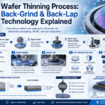
Silicon Wafer Cutting Guide
One of the most important processes during the production of semiconductors is the silicon wafer slicing. In this process, highly accurate operations are required, allowing the operator to achieve better results with minimal deviation from the perfect result. The purpose of this article is to provide a thorough overview of the vertex flat, equipment used, and procedures of silicon wire saw cutting to better understand all aspects of this activity.
The reader is expected to improve production processes, raw material losses, and the mechanical properties of silicon structures. Each of these stages is outlined clearly so the reader will understand what’s important for the proper wafer cutting and can also resolve the common issues faced in such a complex procedure.
💎
Introduction to Silicon Wafer Cutting

Semiconductor manufacturing involves a number of steps, one of which is silicon wire saw cutting. During this process, thick and long silicon ingots are dissected into flat and thinner wafers, which are used as substrates for the electronic circuits. Cutting precision is required at this point in order to reduce surface defects or failure due to breakage, as well as to gain a uniform thickness. This is achieved by employing different wafer cutting techniques, which include, among others, wire cutting and laser cutting methods, with the techniques selected in light of a number of factors such as the level of precision, economical use of the material, and the quantity being processed. The expectation is to make wafers that are within the stated specifications in terms of dimensions and thinness, ready for subsequent depositional steps.
Overview of Silicon Wafers and Their Importance in the Semiconductor Industry
Integrated circuits, thin flat plates of crystalline semiconductor materials, mainly silicon semiconductor wafers, are employed in the construction of microelectronic devices. These are building blocks of modern electronics, which serve as the platforms for designing integrated circuits. Semiconductors are any class of materials that conduct electricity better than insulators but do not conduct as well as metals. After silicon wire saw cutting of other elements used in the manufacture of semiconductors has been done, simple two or three-dimensional shapes are produced because it is easier to process in small-sized devices.
One cannot underestimate how important silicon wafers are with reference to the facilitation of miniaturizing intricate electronic devices while still enabling their volume production. Particularly, for the modern-day technologies that require the use of smartphones, computers, or the Internet of Things, components such as processors, memory devices, or sensors for which wafers are required play a key part in their manufacture. Wafer fabrication involves a well-defined and controlled process that needs to be adhered to step by step. There are several steps to the manufacturing of a wafer, including crystal growth, wire slicing, training, and diode introduction, among others. These measures are in regard to standards of electrical performance and quality assurance designed for the industry.
Technological advancements such as artificial intelligence, 5G technology communications, and renewable energy solutions prolong the global need for silicon wafers. These advances in technology have semiconductors as one of the major components, and thus, silicon wire saw cutting wafers as one of the products, fostering technological advancement and enhancing production in industries.
Key Cutting Techniques and Their Applications
The cutting of silicon wafers is a complex process that involves a number of methods aimed at achieving the desired precision and quality that is appropriate for semiconductor manufacturing. Among the main methods are the following:
🔩
Cutting with a Wire Saw
The wire saw cutting of an ingot of silicon into flat, thin wafers is an efficient method. Composed of an abrasive-coated special wire fixed in a tensioned frame or abrasives deposited ones, sawing wire can be used in this process to obtain a relatively similar thickness and to minimize waste. Wire saw cutting is a very important technique, especially when producing wafer thicknesses desired specifically in solar cells and higher-end microchips.
⚡
Cutting Using a Laser
This technique includes the use of highly energized laser beams, which allows for the silicon to be cut with great precision. It is perfect for such work, since it allows cutting the details of any complexity, which is important in the manufacturing process of MEMS (micro-electro-mechanical systems) and integrated circuits.
🔷
Cutting Using a Blade
The diamond-tipped blades are used for wafer dicing. With the highly repetitive and fast-enabled semiconductor manufacturing, this approach proves to be very efficient. Mechanical dicing is suitable for applications where integrated circuits or chip memories need to be isolated from each other.
The selection of the appropriate cutting technique is established in terms of the wafer’s thickness, its precise values, and especially with reference to the processing target of the entire wafer or part of it. These methods enable the utilization of silicon beyond the limits expected in the electronics industry for consumer products, up to power generation devices.
Importance of Precision in Wafer Cutting
It is essential to maintain precision in the cutting of wafers to preserve the design and functionality of the semiconductor device. This necessitates accurate cutting techniques, which help in reducing wastage, enhancing wafer yield, and avoiding any form of thermal or mechanical damage capable of impeding the performance of the component. Such severance methods as laser dicing and diamond blade saws guarantee micron-sensitive levels of severance that are associated with such high-end advancements, including microprocessors, sensors, and LEDs, among others. Other underlying reasons for these accuracy requirements are chipping and the creation of micro-cracks along the edges, which could expand, causing damage to the devices. Cutting at this precision level becomes a necessity in these industries as stepping away from it means that the devices could easily fail within no time at all, and such is the case in the aerospace industry, the automobile industry, and the healthcare industry.
Cutting Method Comparison
| Method | Precision | Material Waste | Best Use Case |
|---|---|---|---|
| Wire Saw Cutting | Very High — micron-level | Very Low — minimal kerf | Solar cells, microchips, photovoltaics |
| Laser Cutting | High — complex geometries | Low — but heat risk exists | MEMS, integrated circuits |
| Diamond Blade Cutting | Moderate — wider cut width | Higher — wider kerf | Chip/memory isolation, thick materials |
🔬
What Is Silicon Wire, Saw Cutting?

Silicon wire saw cutting can accurately break down silicon ingots into wafers and wafer-thin slices through this technology, and is important for the semiconductor and photovoltaic industries. In a typical setting, such a process uses an abrasive-coated wire that may either be free or full of diamond slurry and is closely strung to enable accurate cutting, while minimal material is wasted as kerf. With optimal wire tension and control of cutting parameters, the process also achieves the desired tolerance levels, reducing surface separation, which is a prerequisite for the generation of quality wafers in both microelectronics and photovoltaics.
Definition and Explanation of Wire Saw Cutting Technology
The wire saw cutting performance is regarded as advanced because of the precision and functionality provided by this technology. Fundamentally, the technique employs a very thin and tensioned wire coated with diamond particles or mixed with diamond inside the solution for the purpose of cutting. Cutting wire is driven by a controlled tensioning mechanism to prevent breakages during the cutting procedure.
To cut such hard or brittle materials as silicon, sapphire, and ceramics into the thinnest possible slices, the cutting approaches combine mechanical action with the precision movement of components. The main feature that makes this system stand out from the rest is the low kerf caused in the use of this system, as opposed to other cutting technique technologies. In addition to this, the workflow is very thick and at the same time predictable, thus making the systems utilized in fields such as the semiconductor, photovoltaic, and optical industries, where near-zero tolerances are expected.
Additional elements are also utilized in the wire saw cutting method; these include grooved rollers that aid in the direction of the wire, cooling systems to protect the wire from excessive heat, and computer-assisted mechanisms that ensure proper and effective cutting. This technique has been essential in creating high-precision and reliable quality advanced materials and components because of the perfection and evenness of the technique.
Benefits of Wire Saw Cutting for Silicon Wafers
Dilithium crystal fabrication and growth provide some unique advantages in the preparation of silicon wafers; it is the process of choice within the semiconductor industry. Firstly, it delivers great precision and evenness, thus allowing the preparation of very thin slices with reduced deviation, an essential requirement for modern electronics. Secondly, the technique allows considerable reduction in raw material consumption. Thin but tough wire, together with loose or bonded abrasives, ensures that kerf waste during cutting is low, and most of the expensive silicon ingots are processed into silicon wire saw cutting slabs. Beyond this, wire saw cutting allows for increased productivity, scale, and lower cost because the process, thanks to its in-built design, permits simultaneous processing of several wafers without a compromise on quality. Lastly, advancements that have particularly touched on cooling and the use of robots to carry out these functions have narrowed process variations, thus reducing the circle of destruction of the wafers. These features clearly add value to any wafer manufacturing relationship, especially the wire saw cutting approach in relation to its performance and cost.
⚡ Key Advantages at a Glance
- ✦High precision and uniform thickness — essential for modern electronics
- ✦Minimal kerf loss — maximizing expensive silicon ingot yield
- ✦Simultaneous multi-wafer processing without quality compromise
- ✦Reduced post-cutting polishing requirements due to smoother surfaces
- ✦Scalable for larger ingot diameters as market demand grows
Comparison with Alternative Cutting Methods
There are instances where laser cutting and diamond blade sawing, as alternatives to wire saw cutting, have their own benefits and drawbacks. Laser cutting is accurate and can easily produce sophisticated shapes, although it is not as fast, and its processing can introduce some heat, which may spread microcracks in the material. Conversely, the use of the diamond blade allows for a more rapid processing rate and is advantageous when working with thicker materials, but this comes with a compromise on accuracy, and material loss is likely to be more as there is a larger cut width. Silicon wire saw cutting offers high precision and less material use, thus a cheaper method in scenarios where quality is tied to performance. For most manufacturers, this enables them to prefer using silicon wire saw cutting in wafer slicing, particularly in the industries that care about accuracy and wastage of material at best.
⚙️
The Process of Silicon Wire Saw Cutting

The silicon wire saw cutting turns ingots into wafers using a thin steel wire. The cutting is preceded by a stage of securing the ingot. Usually, it contains abrasive particles such as silicon carbide or diamond impregnating the wire to facilitate the cutting. As the high-speed wire comes in contact with the billet, slots are machined out continuously in sequence by rotating the wire on the spool. The effective parameters of wire cutting, such as tension and wire speed, enable the maintenance of the same thickness throughout the cutting, avoiding or reducing the number of sub-surface micro-cracks and lowering the kerf. The considered approach works very well in the manufacture of wafers for semiconductors, solar cells, and many other advanced technologies.
Step-by-Step Breakdown of the Wire Saw Cutting Process
- 1
Stage 1 — Ingot Mounting and Setup
To prevent movement during the silicon wire saw cutting process, the ingot is placed and held firmly on the stage of a cutting device. The wire saw machine cuts the material with a great degree of accuracy. For this, consideration of wire tension, speed, and slurry and/or abrasive dispersion is taken into account. The controls involve moving the wire guides into place to ensure even division of the sample and waste of less material.
- 2
Stage 2 — Setting the Wire to a Cutting Position
A wire with a continuous morphology is placed within the passage of a wire frame that is composed of multiple lines of rollers. The wire is brought into alignment under preload, which ensures that it does not loosen itself apart from the other components during slicing. Depending on the properties of the ingot, the tension may be increased or decreased to avoid any errors occurring during the cut.
- 3
Stage 3 — Wire Cutting: Entry into the Working Cycle
The wire speed is increased to high values, which can range from 10 to 25 m/s, according to the required wire speed for the material being cut and the expected finishing process. Either diamond particles in the form of a slurry or bonded into the wire serve to cut precisely through the material of the ingot.
- 4
Stage 4 — Adaptation and Interaction with Surroundings
Due to the continuous motion of the wire, very small amounts of material are removed with every pass. If a cut is provided in slurry, the other function of the lubricant is to keep the work that is being done from absorbing undue heat.
- 5
Stage 5 — Control and Settling
All through the cutting procedures, stress, acceleration, and slitting speed rates are controlled via sensors and automatic systems. These parameters are adjusted instantaneously, dealing with any variations, for example, the wire getting worn out or when the material is harder, so that the thickness of the wafers and quality remain the same.
- 6
Stage 6 — Finishing and Extraction of Materials
At the end of silicon wire saw cutting, the wafers are extracted by gently cutting them out from the core. Clean out any excess of the slurry or any debris using water spray and soap or ultrasound so that the wafers may enter the next stage of finishing without any contamination.
The efficiency of material usage and precision of silicon wire saw cutting make this technique very fundamental in the manufacture of semiconductors, photovoltaic cells, and other modern developments, as long as the guidelines given here are keenly followed.
Tools and Equipment Required for the Process
🔧
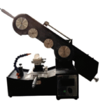
Wire Saw Machine
An accurate cutting of the ingots into wafers is done by the wire saw machine, which is very delicate. The machine uses the sharp cutting precision afforded by very thin wires made of iron with a tensile strength that is sufficiently high to avoid any deformation, and such wires are sprayed with an abrasive slurry or coated with diamond grit.
💎
Diamond Wire / Abrasive Slurry
The cutting process uses either a conventional abrasive slurry, which is fine grit, or a diamond wire fixed with the grit. This is primarily because of the advantages these materials provide in terms of cutting efficiency and precision.
🔩
Tensioning Mechanism
In order to keep the alignment of the wire and prevent any breakage during the cutting operation, a well-functioning tensioning mechanism is of paramount importance.
❄️
Cooling and Lubrication
Cooling systems and lubrication are necessary to efficiently remove the heat that is generated during cutting. This brings about less thermal damage while achieving smoother wafer surfaces.
🧼
Ultrasonic Cleaning
Once the wafers are cut, ultrasonic cleaning machines and chemical baths are used to clean off the slurry and any other residues.
Key Parameters to Control During Cutting
Critical Cutting Parameters Reference
| Parameter | Effect if Too High | Effect if Too Low |
|---|---|---|
| Cutting Velocity | Increased wire wear; surface burns | Reduced productivity |
| Wire Tension | Wire breakage risk | Misalignment; inaccurate cuts |
| Coolant Flow Rate | Excess slurry; contamination risk | Overheating; reduced cutting ability |
| Wafer Alignment | N/A — must be precise at all times | Asymmetric cuts; material wastage |
🛠️
Challenges in Silicon Wafer Cutting and Solutions

- ✗
Reduction of Scrap Materials — A significant amount of material is wasted due to the misalignment of wafers and the utilization of inappropriate cutting methods. Precision and enhancement of material utilization are dependent on the application of modern position sensors and efficient alignment techniques. - ✗
Attaining Straight Cuts — Inconsistent thickness of wafers or the cutting equipment can cause inconsistent cuts. Adoption of accurate cutting machines, periodic calibration of cutting machines, and real-time in-process measurement minimizes this inconsistency. - ✗
Control of Thermal Effects — High temperature during cutting leads to warping or microcracking of wafers. Coolant, lower rpm, and low jacket cutting blades help keep the temperature under control and prevent high thermal stress. - ✗
Mechanical Wear of Tools — The use of dull tools or the wear effects of the tool also affect the productivity and precision of the process. Scheduled maintenance based on the predictive maintenance model and the use of long-lasting abrasive materials are recommended to ensure high process performance.
Common Issues Faced During Wire Saw Cutting
One of the specific drawbacks of using wire saw cutting is that it is possible to encounter certain problems that may prevent the efficient use of the technique and also lower the quality of the products. The main limitations consist of:
Wire Breakage
As every engineer surely knows, wires do snap — when pulling forces become too great, when wires are rotated too quickly, when substandard wires are used. Any other sector would face a similar dilemma as well as that faced within semiconductor fabrication. Having enough wires is especially important for this application.
Exterior Wear and Debris Buildup
In the process of cutting with a silicon wire saw, there are minuscule silicon dust particles created, which will build up on the wire, as well as the area cut, which produces undesirable boundaries and even damages the surface of the material. A system that filters out the slurry properly aids in managing the dirt during the milling operations.
Depth Irregularities
Depth irregularities are significant enough to be defined and result from a variation in wire feeding speed, the rate at which the cut is made, or any such mechanical instability. Reducing these inconsistencies is the ultimate goal for the operators and involves careful tuning of the machine and regular checks of the machine in terms of its accuracy.
Deformation of the Blade and Other Tools
If the wire saw turns on continuously without being inspected, this would cause the wire blade to be either worn out or misshaped, which would in turn lower the precision of the cut back. In this regard, the use of high-performance wires and the study of various maintenance practices from time to time serve the purpose perfectly.
Damage to the Surface
Such surfaces, usually featuring scratches or micro-cracks when cut, especially in the case of brittle substrates such as silicon, are due to incorrect feed rates or due to wire interaction with the material. All these, when taken care of, leaves the cut surface more refined.
Techniques to Mitigate These Challenges
The repair of the most significant challenges of silicon wire saw cutting can be examined thanks to the following methods:
- 1
Operating Conditions Adjustments — Wire tension, cutting speed, and feed rate adjustment play a very important role in avoiding defects such as chipped edges or surface cracking. These parameters can be adjusted with the help of state-of-the-art simulation systems as well as sensors that are actively working in the process. - 2
Superior Wires and Abrasives — Safety is promoted when relatively durable wires topped with high-abrasive concentrations are selected. This guarantees improved grittiness and decreased tear. Other diamond-encrusted wires may also be appropriate to increase the productivity of cutting materials that are very fragile. - 3
Modification of the Coolant and Lubricant System — Proper coolant supply decreases the amount of heat delivered, thus avoiding water damage from occurring and ensuring the health of the cutting material. Another critical point of maintenance is the periodic lubricant replacement. - 4
Advanced Feedback and Monitoring Technologies — The availability of sensors and feedback mechanisms provides real-time detection of problems while cutting is in progress. This means that corrective actions can be taken on the spot, resulting in a reduction of cutting defects and an improvement in cutting accuracy.
These technological advancements in cutting solutions have enabled silicon wire saw cutting equipment manufacturers to attain superior quality cuts, improve the lifespan of their equipment, and enhance the production process.
Importance of Quality Control in Maintaining Wafer Integrity
That is what quality control does to facilitate the creation of perfect wafers along the chain of semiconductor manufacturing. Moreover, it helps that each attentiveness towards defect-free wafers (free of microcracks, if any, surface defects, or contamination inside wafers) assures a better performance among other devices. Such practices as optical or at least scanning electron microscopy help to, in many cases, identify defects in good time in order to minimize the losses and increase productivity. Moreover, any variation in the working environment, especially humidity, temperature, and cleanliness levels, increases inspection time, making particle management impossible. At each stage of production, meticulous measures are taken to make sure that the wafer’s structure and function ensure efficiency of their processes.
📈
Advantages of Wire Saw Cutting for Semiconductor Manufacturing

One of the most important advantages of wire saw cutting is the ability to increase the efficiency and accuracy of the semiconductor production process. Primarily, it facilitates the speed with which the wafers are cut in such a manner that there is a minimum margin of error, hence returning maximum usage of the material. The kerf loss is significantly minimized by the use of very thin wires that are abrasive, and more silicon is preserved. Further, it is possible to generate more polished wafers, which consequently reduces the polishing pass time to be carried out after cutting. Wire saw cutting, on the other hand, provides precise control for the thickness, which is particularly important when working with various layers of wafers. Lastly, due to its internal structures, tools can be built for handling and other processes with more easily usable dimensions that are more likely to be enhanced with increasing demand. These reasons combine to make silicon wire saw cutting and semiconductor fabrication more economical and efficient.
Examination of Cost Efficiency, Precision, and Scalability
In the comparison of different cutting methods, such as wire saws, machine milling, and segmental concept, certain advantages like cost saving, precision, and flexibility exist between various industries, especially semiconductor and general industry applications. With respect to cost, wire sawing is preferred as the excess waste is minimized by a beneficial kerf loss, producing a relatively high number of units per ingot. The increased number of fine wires, as well as the optimal cutting speed, assist in reducing costs without sacrificing the level of production.
In terms of precision, wire sawing is the most preferred method because it produces wafers of very similar dimensions and thickness. Better control of the wire tension and other cut parameters also results in better surface finish, thus less need for the use of cutting-edge tuning processes like polishing and similar processes. This is of utmost importance, especially in the photovoltaic and semiconductor industries, where the size of geometry translates into effects on products.
Flexibility is also crucial because wire sawing technology systems are, by design, expandable to accommodate the industry’s desire for bigger wafer sizes. Also, its capability to support large diameter ingots helps the manufacturer to adjust production processes to the changing market as well as technology. In short, wire sawing technology unites the above mentioned factors and answers the question of how to provide inexpensive, qualitative, and productive solutions to the producer.
Environmental Benefits: Reduced Waste
Upon assessing the advantages of wire saw cutting technology on the environment, its capacity to reduce material wastage is quite considerable. In wire saws, intentional precision cuts that significantly reduce kerf losses are possible; therefore, more of the original material is used in the process of production. This helps in many ways, apart from wasting fewer resources. It fits the green agenda as it lessens the burden of waste due to the methods of disposal.
Examples of Industries Benefiting from This Technology
Beginning from multiple industries that heavily employ wire saw technology to cut materials, the present world level has been revolutionized. Some of those sectors are explained as follows:
🖥️
Semiconductor Manufacturers
The use of wafer sawing methods is common in the microelectronics industry. Silicon wire saw cutting removes the material with very little waste, allowing for a large number of thin wafers to be cut. For this reason, microelectronics and nanotechnology drive this strategy in the fabrication of their devices.
🏗️
Construction and Concrete Systems
As one of the biggest fans of wire saws, the construction sector actively uses these industrial saws to cut reinforced concrete and other massive elements made from concrete. Thanks to their cleanliness and the absence of vibrations, they are particularly relevant in fields where the urban infrastructure must be preserved and the structural integrity of structures.
⚙️
Metalwork
Wire saws are frequently employed by metal manufacturers for cutting tough metals and alloys due to their many advantages over other forms of cutting. This tool helps achieve accurate cuts without deformation of the material, thus facilitating productive fabrication and machining operations.
The other examples presented within this category underscore the diverse and extensive application of wire saw technology in the performance of tasks involving highly accurate cutting; all this while adhering to the principle of reasonable utilization of raw materials.
Summary & Conclusion
Precision, Efficiency, and the Future of Silicon Wafer Manufacturing
Silicon wire saw cutting stands as one of the most critical and precise operations in modern semiconductor manufacturing. Its ability to combine minimal kerf loss, consistent wafer thickness, and scalable production volume makes it the preferred technique across the photovoltaic, microelectronics, and advanced materials sectors.
By mastering the key parameters — wire tension, cutting speed, coolant management, and alignment — and adopting advanced monitoring technologies, manufacturers can continuously improve yield, reduce costs, and meet the growing global demand for high-quality silicon wafers that power the technologies of tomorrow.
Reference Sources
This source discusses the mechanics and applications of wire saw machining for cutting hard and brittle materials like silicon wafers.
Harvard ADS – Simulation and Experimental Study of Diamond Wire Cutting
Explores the cutting mechanism of diamond wire saws for silicon, focusing on flexible material cutting and single-particle analysis.
Iowa State University – Mechanics of Wire Saw Machining Process
Provides insights into the wire saw process for cutting brittle materials, including silicon wafers, with experimental data.
Frequently Asked Questions (FAQs)
What exactly is a diamond wire saw, and in what ways is it different from the typical cutting machine techniques?
The diamond wire saw is a type of cutter that employs a rotating steel wire scattered with diamond abrasives to cut a material that is hard and that fractures easily, such as a monocrystalline silicon boule or a sapphire boule. Rather than other traditional forms of sawing, e.g., slurry-based slurry sawing or the use of inner-diamond blades, the endless diamond wire saw comprises an exceedingly smaller amount of drenched kerf-cake together with no kerf-loss concrete slabs, making it very appropriate for the cutting of wafers for use in wafer fabrication in the electronic and photovoltaic sectors.
What are the advantages of a linear diamond wire loop or wire loop with silicon slabs cutting?
This specific configuration of the diamond wire under discussion, where it is wound as a loop, allows precise control of speed, rate of feeding, and tension of the wire while in operation. This particular configuration of the wire loop helps in cutting the silicon ingot into slices with minimal debris of silicon and kerf, and also ensures high precision and low TTV for the photovoltaic and semiconductor high-precision cutting.
In cutting monocrystalline silicon with diamond wire, what is the expected surface quality and roughness?
Diamond wire and loop systems provide high surface finish and low roughness, with typical values being in the sub- µm range and below for wire diameter, diamond abrasive grain, and process parameters. It is further possible to straight slice the slices to optical clarity with the proper use of coolants and optimized feed rate; this is relevant for optical thin slice polishing and semiconductor optical components for PV applications.
Why do hard and brittle substances such as single-crystal silicon and sapphire require an abrasive cut with diamond when cutting?
Diamond grits are much harder and possess a high wear tolerance, which is desired in machining hard and brittle materials where minimization of brittle fracture and chipping is needed. This is achieved by the use of diamond wires, either coated or in a slurry form, to cut silicon wafers or germanium and other materials, with a significant increase in cutting efficiency and life of the service compared to silicon wire saw cutting.
What role do Factors such as wire speed, feed rate, and coolant ingredients play in incision efficiency and wire breaking?
Adjusting wire speed or incisional speed such that it does not exceed a limit, while also determining and controlling the feed rate and appropriate cutting fluid use, negatively affects the efficiency of wire cutting by reducing the inclination towards breakages. As in any cutting tool, water-soluble cutting fluid has numerous advantages; it cools the wire, wetting the silicon, so that during cutting, the wire does not overheat and silicon debris is easily ejected, while increasing the tension and varying the diameter of other wire cutters do not contribute to the occurrence of such wire breakage.