Get in touch with DONGHE Company

Quick Specs: The Equipment Landscape at a Glance
| Process steps per chip | 300+ steps (USITC) |
| Distinct equipment types | 50+ (USITC) |
| Two main segments | Front-end (wafer fab) + back-end (assembly, test, packaging) |
| Front-end share of spend | ~80% of equipment capex (≈$108B of $135.1B, 2025) |
| Cleanroom class | ISO 14644-1 Class 1–5 |
| First machine to touch the crystal | Diamond wire saw (ingot slicing) |
What Is Semiconductor Manufacturing Equipment? The 8-Stage Equipment Stack

Semiconductor manufacturing equipment (often shortened to SME or “semiconductor production equipment”) is the family of precision machines that fabricate integrated circuits on semiconductor wafers. A wafer is a thin, polished disc of semiconducting material, usually silicon, sometimes silicon carbide or sapphire, that serves as the substrate on which thousands of identical chips are built in parallel. Because each chip is patterned at near-atomic scale, every machine in the chain has to operate inside a contamination-controlled cleanroom.
It helps to group the 50-plus equipment types into four broad families: wafer-shaping tools (crystal growth and slicing), front-end wafer-processing tools (lithography, deposition, etch, ion implantation, chemical mechanical planarization), back-end tools (dicing, bonding, packaging, test), and metrology and inspection tools that police quality at every step. This master map anchors the rest of the guide.
| Stage | Equipment category | What it does | Key metric |
|---|---|---|---|
| 1. Crystal growth | Czochralski / float-zone pullers | Grow the single-crystal ingot | Ingot diameter (up to 300mm) |
| 2. Wafer slicing | Diamond wire saw / multi-wire saw | Slice the ingot into wafers | Kerf, TTV |
| 3. Patterning | Lithography (DUV / EUV) scanners | Print circuit patterns | Resolution (nm) |
| 4. Deposition | CVD / PVD / epitaxy / ALD | Add thin films | Film thickness uniformity |
| 5. Etch | Plasma / wet etchers | Remove material selectively | Etch selectivity |
| 6. Doping + planarization | Ion implanters / CMP tools | Tune conductivity, flatten layers | Dose, surface flatness |
| 7. Dicing + packaging | Dicing saw / laser / bonders | Singulate and package die | Dicing kerf, bond yield |
| 8. Metrology + test | Inspection tools / wafer probe / ATE | Measure and grade quality | Defect density, yield |
Synthesis of process-step taxonomy from semiconductor device fabrication documentation and USITC equipment categories.
One thread run through all eight stagesyield: every machine either protect or erodes the percentage of working chips you get from a wafer. That’s why the order matters, and why the wafer that get sliced in stage 2 quietly sets a ceiling on everything that follows. For the full step-by-step flow, see our companion guide on the semiconductor manufacturing process.
Front-End vs Back-End: The 80/20 Fab-Equipment Rule

One split organizes semiconductor manufacturing equipment more usefully than any other: two halves. Front-end (wafer fabrication) tools build the circuits onto the wafer. Back-end tools take the finished wafer and turn it into individually packaged, tested chips, assembly, test, and packaging (ATP). Both the USITC and every fab budget use exactly this split.
Here’s the rule worth remembering: roughly 80% of equipment spend is front-end, and roughly 20% is back-end. Global equipment billings hit $135.1 billion in 2025 (SEMI), and the front-end wafer-fab-equipment slice alone was about $108 billion. That weighting is why a single lithography scanner can cost more than an entire back-end line, but, as the trend section show, the 20% is where growth is now fastest. For a buyer, the practical risk is mis-budgeting: teams that treat the back-end 20% as trivial get blindsided when a test or packaging tool, not a scanner, becomes the line’s bottleneck. A planner who maps spend to this split early avoid ordering front-end tools on time while a back-end machine with a longer lead time quietly sets the ramp date.
| Dimension | Front-end (wafer fab) | Back-end (assembly/test/packaging) |
|---|---|---|
| Job | Build circuits on the wafer | Singulate, package, and test the die |
| Example tools | Lithography, deposition, etch, implant, CMP | Dicing saw, wire/hybrid bonder, molding, test (ATE) |
| Approx. capex share (2025) | ~80% (~$108B) | ~20% |
| Momentum | Large, steady | Fastest-growing (test +48% in 2025) |
“The entire fabrication process can require over 300 steps utilizing over 50 different types of semiconductor manufacturing equipment.”
U.S. International Trade Commission, The Health and Competitiveness of the U.S. SME Industry
Front-End Equipment: Lithography, Deposition, Etch, Implant and CMP

Front-end equipment does the actual circuit-building, and it clusters into five core categories. Each one is repeated dozens of times across the 300-plus process steps, layer after layer.
What tools are used in semiconductor manufacturing?
Core front-end tools are lithography scanners, deposition systems, etchers, ion implanters, and chemical mechanical planarization (CMP) polishers, plus the cleaning and metrology tools between them. Semiconductor Engineering describes a modern node as “a number of different process steps, such as lithography, etch, deposition, cleaning, CMP, doping.” In practice:
Pain for a new fab is rarely the price tag; it’s lead time. Semiconductor Engineering reports demand and lead times soaring for 300mm equipment, so the scarce resource an engineer fights for is tool delivery, not capital. Picture a process engineer qualifying a new etcher: it must match the deposition step before and the CMP step after, or yield drops across the whole module.
- ✔ Photolithography (DUV/EUV): prints the circuit pattern. This is the costliest single tool classa High-NA EUV scanner carries a price tag of more than $400 million.
- ✔ Deposition, chemical vapor deposition (CVD), physical vapor deposition (PVD), epitaxy, ALD: grows thin conductive and insulating films.
- ✔ Etch, plasma etching and wet etching: removes material selectively to define features.
- ✔ Thermal processing (annealing): activates dopants and relieves stress between layers.
- ✔ Ion implantation: dopes the silicon to set its electrical behavior.
- ✔ CMP (chemical mechanical planarization): polishes each layer flat before the next is built.
📐 Engineering Note
Lithography sets the headline “node” (e.g., 3nm), but resolution is meaningless if the wafer underneath it isn’t flat. CMP and front-end inspection exist precisely to preserve the planarity and pattern fidelity that the scanner assumes, inline process control keeps surface roughness inside spec layer after layer. A wafer that arrives from slicing with poor total thickness variation (TTV) forces extra CMP passes, extra cost, extra defect risk. That same front-end line builds everything from logic chips to a discrete power device or a MEMS sensor, each an integrated circuit patterned on the same wafer.
Wafer Shaping and Slicing Equipment: From Ingot to Wafer

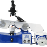
Before a single transistor exists, a machine has to turn a cylindrical crystal into hundreds of thin, flat wafers. That machine is a silicon wafer cutting wire saw. Step by step: grow the ingot (Czochralski or float-zone), crop and grind it round, then slice it with a diamond multi-wire saw that runs hundreds of parallel wires through the crystal at once. Lapping, edge-grinding, and polishing follow.
This is the stage most equipment guides skip, and it’s the one that quietly governs yield. Two numbers decide everything downstream: kerf (the material lost to the cut) and TTV (total thickness variation across the wafer). A wafer that’s sliced unevenly can’t be fully recovered later, the front-end simply inherits the error. In our own cutting-case database of 10,000-plus jobs across 50-plus materials, the slicing recipe (wire speed, tension, feed rate) is the variable that most often separates a high-yield wafer from a scrap one.
| Parameter | Multi-wire series | Single-wire series | Loop-wire series |
|---|---|---|---|
| Wire diameter | 0.04–0.6mm | 0.04–0.65mm | 0.35–2.2mm |
| Max wire speed | 3000 m/min | 1800 m/min | 60–84 m/s |
| Slice thickness | ≥0.04mm | Custom | N/A (profile cutting) |
| Kerf (achievable) | as low as 60µm | as low as 60µm | application-dependent |
Source: DONGHE machine specifications (positioning accuracy ±0.001mm, repeatability 99.9%, sub-micron TTV).
For a deeper look at how the cut itself work, see how a diamond wire saw works, and for the substrates being sliced, our overview of silicon wafer material.
Back-End Equipment: Dicing, Bonding, Packaging and Test

Once the wafer is fully processed, back-end equipment turns it into shippable chips. Each wafer is diced into individual die, the die are bonded and packaged, and every unit is tested afterward. Back-end tooling used to be treated as the cheap afterthought, that framing is now wrong, and the dicing choice is a good example of why.
What machines are needed to make semiconductors?
Beyond the front-end fab tools, you need back-end machines: a dicing saw or laser dicer to singulate the die, die bonders and wire/hybrid bonders to attach and interconnect, molding and encapsulation equipment to package, and automated test equipment (ATE) plus a wafer probe to grade performance. Dicing alone carries real trade-offs:
| Method | Typical kerf | Best for | Watch-out |
|---|---|---|---|
| Blade (saw) dicing | ~27µm | Standard silicon, thick die | Chipping on brittle/thin wafers |
| Laser dicing | ~15.4µm | Ultra-thin wafers, tight streets | Heat-affected zone; not ideal for thick Si |
| Plasma dicing | very narrow | High die-count, small die | Needs mask + etch infrastructure |
Kerf figures per Semiconductor Engineering.
⚠️ Common Misconception: “laser dicing is always better”
Narrower kerf does not make laser the default. Practitioners cutting silicon wafers routinely report that, for many jobs, “laser is the wrong tool — a diamond saw is preferred,” with lasers reserved for shapes a saw cannot reach. This frontier is increasingly hybrid: USPTO-published methods such as US8853056B2 combine femtosecond laser scribing with plasma etch precisely because no single method wins on every material and thickness.
Metrology, Inspection and Test Equipment

Metrology and inspection equipment never adds a feature to the chip, it decides whether the features already there are good enough to continue. This is how fabs protect yield in real time rather than discovering scrap at final test. Three classes matter:
- ✔ Inline metrology: film-thickness, overlay, and TTV/flatness measurement that flags drift before a whole lot is lost.
- ✔ Defect inspection: optical and e-beam tools that hunt particles and pattern defects, the reason fabs hold ISO 14644-1 Class 1 cleanrooms.
- ✔ Electrical test: a wafer probe checks die on-wafer; automated test equipment (ATE) grades the packaged part.
Practical takeaway: when you read a TTV or kerf spec on a slicing machine, that number is what the metrology tools 200 steps later will measure against. Quality is set early and verified late.
Who Makes Semiconductor Manufacturing Equipment?

Semiconductor manufacturing equipment is built by a concentrated set of specialist suppliers, each dominating one process step rather than the whole line. No single vendor makes every tool, so a fab assembles its line from several segment leaders: lithography from one supplier, deposition and etch from another, slicing and dicing from a third.
Who is the largest semiconductor equipment manufacturer?
By revenue, Applied Materials is generally the largest semiconductor equipment manufacturer, followed by ASML and Lam Research. This market is highly segmented, though, each tool category has its own dominant suppliers, and “largest overall” is different from “must-have for a given step.” USITC analysis documents this front-end/back-end segmentation across equipment makers. This table maps the major equipment segments to the companies most associated with them (named here as market context, not as a recommendation).
| Segment | Representative suppliers |
|---|---|
| Lithography | ASML (EUV/DUV), Nikon, Canon |
| Deposition + etch | Applied Materials, Lam Research, Tokyo Electron |
| Metrology / inspection | KLA |
| Dicing / back-end | DISCO, ASM Pacific |
| Wafer shaping / slicing | Diamond wire saw specialists (incl. DONGHE) |
For buyers, the more useful question is rarely “who’s biggest” but “which supplier owns the step I’m sourcing.” A fab doesn’t buy “a semiconductor equipment company”; it buys a scanner from one vendor, a slicing machine from another, and a tester from a third. A common procurement mistake is shopping for a brand instead of a step: a team sourcing a wafer-slicing machine and a team sourcing an EUV scanner are in entirely different markets, with different lead times, spare-parts supply, and after-sales engineering. From our own experience supplying the wafer-slicing segment, the vendor who owns your exact process step, and can tune the recipe to your material, matters far more than overall revenue rank. A buyer who skips a test cut to save a week often pay for it in scrapped wafers later.
How to Choose Wafer Slicing and Dicing Equipment

If you’re actually specifying a cutting machine, for slicing ingots or dicing wafers, the deciding variable is the material, because hardness and brittleness drive the wire, kerf budget, and cutting mode. Use the selector below as a starting point, then validate with a test cut on your own geometry.
| Material | Recommended method | Machine class | Why |
|---|---|---|---|
| Silicon (Si) | Diamond multi-wire slicing | Multi-wire saw, wet | Highest throughput at low kerf |
| Silicon carbide (SiC) | Diamond wire, slow feed | SiC wafer cutting saw | Extreme hardness; protect wire life |
| Sapphire | Diamond wire, controlled tension | Single-wire saw | Brittle; minimize subsurface cracking |
| GaN / thin power die | Laser or hybrid dicing | Laser dicer | Thin, fine streets favor narrow kerf |
✔ Diamond wire saw — advantages
- Lowest kerf loss on hard/brittle materials
- Multi-wire = many slices per pass (throughput)
- Sub-micron TTV with closed-loop tension control
⚠ Limitations
- Consumable wire wear adds running cost
- Not suited to ultra-thin die singulation (use laser)
- Requires coolant management for wet cutting
Dry vs wet is the last call: wet cutting (water-based coolant) handles heat and prolongs wire life for hard materials like silicon and sapphire, while dry cutting suits materials that can’t be wetted, such as certain ceramics and graphite. For photovoltaic-grade slicing, see our diamond wire saw for photovoltaic applications, and to compare substrates first, our guide to types of semiconductor wafers.
Industry Outlook: Reshoring and the Advanced-Packaging Shift

One decision should shape an equipment buyer’s next two years, and it isn’t the headline market-growth number, it’s where capacity is being built and which segment is tightening. Two forces dominate. First, reshoring: U.S. policy under the CHIPS Act and the Advanced Manufacturing Investment Credit has driven over $640 billion in announced semiconductor supply-chain investments (SIA). Second, the advanced-packaging shift: as transistor scaling slows, more performance now comes from how die are stacked and bonded, which is pulling demand toward back-end tools.
What this means for buyers is concrete. Back-end and test capacity, historically the cheap 20% — is where lead times tighten first: SEMI reported test equipment sales surged about 48% in 2025, the fastest-growing segment. CSET (Georgetown) argues advanced-packaging capacity is now a strategic bottleneck, and new fabs prove the point in their schedules: TSMC’s second Arizona fab finished construction ahead of an equipment-installation window, because tool lead times, not concrete, gate production. For context, market researchers project the equipment market continuing to grow at a double-digit CAGR through the mid-2030s, but treat those figures as directional background; the actionable signal is segment timing, not the aggregate curve. Practically: if you source slicing, dicing, or compound-semiconductor (SiC/GaN) cutting capacity, plan tool procurement earlier than the front-end rule of thumb would suggest. Picture a fab planning a 2027 ramp: the concrete is poured on schedule and the cleanroom is certified, but the line waits on a back-end or slicing tool with a 12-month lead time, the classic mistake of budgeting capital before booking delivery slots. Risk is no longer cost; it’s queue position.
Frequently Asked Questions
Q: Who is the largest semiconductor equipment manufacturer?
View Answer
By annual revenue, Applied Materials is usually ranked the largest semiconductor equipment manufacturer, with ASML and Lam Research close behind. But the market is segmented by tool type: ASML is effectively the sole supplier of EUV lithography scanners, while KLA dominates metrology and DISCO leads dicing. “Largest overall” and “essential for a specific step” are different questions, so most fabs buy from several vendors, matching each supplier to the step it owns rather than to one brand.
Q: What is the difference between front-end and back-end equipment?
View Answer
Front-end (wafer fabrication) equipment builds the circuits onto the wafer — lithography, deposition, etch, ion implantation, and CMP. Back-end equipment turns the finished wafer into packaged, tested chips — dicing, bonding, packaging, and test. Front-end accounts for roughly 80% of equipment spending, but back-end is growing faster.
Q: How much does semiconductor manufacturing equipment cost?
View Answer
It ranges enormously by tool. A High-NA EUV lithography scanner can exceed $400 million per unit, while many back-end and wafer-shaping machines cost a small fraction of that. At industry scale, total global equipment billings reached $135.1 billion in 2025. Because pricing depends on the process node, throughput, and configuration, treat any single figure as indicative and request a quote for your specific tool and volume; a leading-edge fab can need tens of billions in tools overall.
Q: Is wafer slicing a front-end or back-end process?
View Answer
Wafer slicing is wafer-shaping, and it happens before any front-end processing begins, turning the grown ingot into bare wafers with a diamond wire saw. Dicing, by contrast, singulates the finished processed wafer into individual die and is a separate back-end step.
Q: What materials can this equipment process?
View Answer
Common substrates include silicon, silicon carbide (SiC), sapphire, gallium nitride (GaN), and quartz. Each has different hardness and brittleness, so each needs its own cutting wire, kerf budget, feed rate, and dry-or-wet mode; a recipe tuned for silicon will not slice SiC well.
Q: Do you need a cleanroom for all semiconductor equipment?
View Answer
Front-end wafer processing demands the strictest environments — modern 300mm fabs run at ISO 14644-1 Class 1, because a single particle can ruin a die. Wafer-shaping and some back-end steps are less sensitive but still controlled. As a rule of thumb, the closer a step is to patterning sub-nanometer features, the cleaner the room has to be.
About This Analysis
DONGHE (Shanghai Donghe Science and Technology Co., Ltd.) designs diamond wire saw machines for slicing silicon, SiC, and sapphire. The wafer-slicing and dicing figures in this guide, kerf as low as 60µm, sub-micron TTV, and the material selector, come from our own machine specifications and a database of 10,000-plus cutting cases across 50-plus materials. The front-end and market figures are attributed to third-party sources below. Reviewed by the DONGHE technical team.
References & Sources
- The Health and Competitiveness of the U.S. SME IndustryU.S. International Trade Commission
- Global Semiconductor Equipment Billings Reached $135.1 Billion in 2025SEMI
- Semiconductor Supply Chain InvestmentsSemiconductor Industry Association (SIA)
- Re-Shoring Advanced Semiconductor PackagingCSET, Georgetown University
- Semiconductors and the CHIPS Act: The Global ContextCongressional Research Service
- 300mm Wafer Fab Contamination Control (ISO 14644-1)University of Texas at Dallas
- Semiconductor device fabricationWikipedia
- Laser Ablation Dicing vs Blade Dicing (kerf data)Semiconductor Engineering
- Wafer dicing using femtosecond-based laser and plasma etch (US8853056B2)USPTO / Google Patents