Get in touch with DONGHE Company

📐 Quick Specs — Semiconductor Multi Wire Saw
| Wire Count | 500–2,000 parallel wires per run |
| Wire Speed | 10–25 m/s |
| Wafer Output | 300+ slices per single cut cycle |
| Kerf Loss | 150–250 µm (standard diamond wire) |
| TTV | <10 µm standard, <5 µm achievable |
| Materials | Si, SiC, sapphire, GaAs, GaN, quartz, ceramics, graphite |
What Is a Semiconductor Multi Wire Saw and How Does It Work?

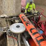
A semiconductor multi wire saw is a precision machine, working on hundreds of parallel thin wires stretched across a set of grooved guide rollers to simultaneously slice a single ingot into a multitude of wafers. A multi-wire saw differs from a single-wire saw — which produces 1 wafer at a time — a multi-wire saw can contain between 500-2000 wire spans in a single wire web, producing 300 or more slices per cycle.
How a multi-wire saw works is simple. A continuous wire (diamond coated or bare wire fed with abrasive slurry) is looped around one or more wire guide rollers, forming a parallel “web” of sawing wires across the workpiece. The ingot is held down onto the wire web by a feed table utilizing an epoxy adhesive to securely mount it. Feed rate is controlled, and as the wire web proceeds at rates between 10-25 metres per second, the wire abrasively wears its way through the workpiece to produce wafers with uniform characteristics, and little wasted material.
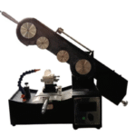
Five core components define the machine architecture:
- Wire guide rollers – the precision-ground cylinders with micro-grooves directing the wire pitch (accuracy ±2 µm)
- Wire web – the array of parallel cutting wires and correctly tensioned wires within
- Feed table – the table which holds the workpiece and presents feed rates as low as 0.2mm per minute (silicon)
- Coolant system – supplying temperature-controlled fluid to the cut zone, washing away debris and removing thermal load
- Tension control unit – ensuring consistent tension across all the wire spans to avoid sagging or breakage
This parallel cutting technique is the common principle to all wedge slicing technology; this characteristic that makes multi wire wire sawing the recognised industry standard in both semiconductor manufacturing and solar cell production.
Diamond Wire vs. Slurry: Two Cutting Methods Compared

For semiconductor manufacture single-wire saws use between 4- 6 hours to slice a 200 mm ingot which produces one wafer. A multi-wire saw performs this entire cycle simultaneously to produce hundreds of slices in the same timeframe.
| Parameter | Slurry Wire Saw | Diamond Wire Saw |
|---|---|---|
| Kerf Loss | 160–200 µm | 120–180 µm |
| Cutting Speed | 300–400 wafers/hr | 700–1,000 wafers/hr |
| Wire Diameter | 100–160 µm (bare wire) | 60–120 µm core + diamond coating |
| Surface Finish (Ra) | Smoother (<0.3 µm typical) | Slightly rougher (0.3–0.5 µm) |
| Environmental Impact | SiC slurry waste (hazardous disposal) | Water-based coolant (recyclable) |
| Best For | GaAs, InP, optic glass | Si, SiC, sapphire |
There are two main methods of wafer slicing using a single wire or a larger number of thinner wires: diamond wire sawing, DWS and slurry based wire sawing, SWS. The following table is a comparison of the two based on real production data.
DWS is now cited as the premier technology for silicon and silicon carbide wafer manufacture. It has been demonstrated in the paper published in Procedia Manufacturing that DWS offers a more sustainable alternative to slurry based cutting, in giving significantly less material wastage and a minimised environmental impact. So compared to slurry based cutting, the higher productivity (2-3x faster throughput) and lower kerf loss can translate directly into vastly more wafers being gleaned from each ingot’s worth of precious semiconductor raw material. This has to be a lucrative benefit.
✔ Diamond Wire Advantages
- 2–3× higher productivity than slurry
- Lower kerf loss = more wafers per ingot
- Water-based coolant (no hazardous slurry waste)
- Required for hard materials: SiC, sapphire
- Compatible with thinner wire for material savings
⚠ Diamond Wire Limitations
- Higher per-meter wire cost vs. bare steel wire
- Rougher surface may require additional lapping
- Not ideal for soft III-V compounds (GaAs, InP)
- Risk of wire breakage increases with SiC hardness
- Diamond grit wear requires monitoring (DWMS recommended)
Slurry based cutting remains the dominant method used for component semiconductors. GaAs and InP are softer and more fragile than silicon, and the free-abrasive action of slurry produces less subsurface damage on these materials. For optic glass applications, slurry also delivers the smoother surface finish required to reduce post-cut polishing steps.
Key Specifications That Affect Wafer Quality

DONGHE offers multi wire saw equipment supporting both applications, slurry and diamond wire.
📐 Engineering Note — Critical Wafer Specifications
- Total Thickness Variation (TTV): <10 m is the standard target of production. Tridirectional high-precision multi-wire achieve <5 m (approaching the wire-EDM benchmark specification). Guide roller quality and wire tension balance will primarily control TTV.
- Bow and Warp: 30 m in typical for 150250 mm wafers. Excessive bow will often result from an imbalance in thermal load during cutting, or residual stress following high feed rate.
- Kerf Loss: 150250 m associated with usual diamond wire. The experimental 50 m thin wire based multi-wire system has demonstrated 100 m kerf loss. However, it has not been commercialized.
- Subsurface Damage (SSD): Approximately 1-30 m depending on the material, wire grit and feed rate. According to the research provided by the PMC/NIH and Springer, small amount of SSD is discovered to be uncontrollable in wire sawing-it can only be minimized and completely removed by process control of the cutting parameters subsequent lapping and polishing.
- Surface Roughness (Ra): It is possible to reduce below 0.5 m before lapping. Diamond wire roughness values are around 0.3-0.5 m. slurry wire roughness values were observed between 0.2 m and 0.3 m.
Uniformity of wire tension (beyond the entire wire web) is the single most important factor affecting the wafer quality. Using wire force measurement in a closed-loop tension control system, the tension along the entire wire web should be measured and regulation with the wire elongation and thermal changes is conducted. Otherwise, the thickness variation between ends of the wire web can be usually over 20 m (which is well outside the SEMI M1 specification in polished silicon wafer category).
When selecting a diamond wire saw to slice semiconductors, it is important to check that the machine has a closed-loop tension control system, a coolant that is controlled to within 0.5 C and guide rollers with pitch accuracy of less than 2 m.
Materials a Multi Wire Saw Can Process

Multi wire saws are versatile equipment designed for cutting many of the hardest and most difficult to machine items in the space of engineering, electronics, photovoltaic processing, and advanced ceramics industry. Items listed below are the principal application modules and materials.
- Silicon (mono- and polycrystalline) silicon is the basis of solar cells and semiconductor wafers. Both mono- and poly- silicon ingots are specified as standard.
- Silicon carbide (SiC) power semiconductors and electric vehicle inverters. The extremely hard nature of SiC (Mohs 9.5) places diamond wire as the only suitable cutting wire. The market analysts forecast that the demand of SiC wafers will grow from 1.69 billion US dollars in 2025 to 6.4 billion US dollars in 2032 with a CAGR of 21.3%.
- Sapphire substrates & optical windows. Diamond wire required in the abrasive due to Mohs 9.
- Gallium nitride(GaN) RF devices power electronics & compound semiconductors.
- Gallium arsenide(GaAs) optical & telecom transmissions. Usually cut with slurry wire in order to reduce surface damage.
- Quartz — optical components and resonators.
- Technical ceramics alumina, zirconia, piezo-ceramics industrial, medical.
- Graphite — electrodes and crucible components.
- Optic glass — precision lenses and prism blanks.
Rising demand for SiC in EV power modules and GaN in 5G infrastructure has induced more and more multi-wire saw equipment being implemented for these applications. Machines offered by DONGHE are all configured for silicon, SiC, sapphire and ceramic processing, with wire tension and feed rate adjustment possibilities for each type of materials.
Common Challenges and How to Solve Them

Wire saw cutting at production scale introduces three common problems. Each is easily diagnosed with known root causes, against which engineering solutions can be tested.
1. Wire Breakage
Wire breakage. Occurs when wire snaps, immediately stopping the cut within seconds, to ruin the entire batch. Sources include tension spikes, caused by worn drive belts, misaligned flow of coolant at wire entry, or wire fatigue due to heating and kinking. Research on wire-saw wear-out effects (PMC) states that as diamond grit is depleted, the rate of wear follows a proportional curve-using count of the number of inches cut by the wire on a given run, portions of the wire can be scheduled out before catastrophic failure.
Solutions: Install a diamond wire management system (DWMS) to measure wear real-time. Cut with lower entry feed rate for first 5 mm of depth. Check drive belt tension every 3 months. Record wire tension and log any spikes greater than 5% of setpoint.
2. Subsurface Damage (SSD)
Sub-surface damage (SSD). Occurs when micro-cracks extend underneath the top surface of the wafer by 1-30 m. Contributing factors include excess feed rate, coarse diamond grit, and vibration. Subsequent electronics processing requires extra grinding, lapping and polishing, leading to higher costs and lower yields if the damage layer becomes too deep.
Solutions: Reduce feed rate when cutting brittle materials (SiC and sapphire). Use grinders with finer grit size (10-20 m to finish cut, 30-40 m to rough cut). Ensure cooling water flow is optimal to reduce vibration and thermal strains. Industry practice states SSD below 5 m is feasible on Si.
3. Inconsistent Wafer Thickness
Variation in thickness across a batch might be caused by expansion of wire web and guide rollers, uneven distribution of wire tension across many pulls, or groove wear in the guide rollers. Thermal drift over 8-10 hours of continuous cut might shift the top surface by 5-10 m.
Solutions: Cool with temperature-controlled coolant to 0.5 C accuracy. Use closed-loop wire tension control, with multiple gauge points distributed across the wire. Schedule monthly measurement and regrinding of roller grooves. Rotate wire after every 8-10 hours of active cutting.
💡 Maintenance Pro Tip
Preventive maintenance schedule: daily wire tension check; drive belt inspection every 3 months; roller groove measurement every month; wire rotation every 8-10 hours. This schedule can reduce unplanned downtime by 30-40%, based on empirical data from factory operations.
How to Choose the Right Multi Wire Saw

Click here to use a checklist to decide what specifications you should choose for your multi wire saw machine.
✔ Selection Checklist:
- Material type – dictates wire type, grit size and feed rate range. Sapphire and silicon carbide need dedicated diamond wire; GaAs can require slurry cutting capacity.
- Wafer size – machine sizes are rated for 150 mm, 200 mm or 300 mm maximum wafer diameter. Confirm your cooling and washing stations fit the selected specification.
- Production volume – R&D groups need machines that cut singular ingots with minimal setup. Production groups require fully automated machines with high throughput and high consistency.
- Machine must support both silicon and III-V cutting wires and slurry cutting if you process both.
- Auto HMI – automated recipe control and equipment messaging network (SECS/GEM) are standard for production environment.
- Spot buy assesses nominal part cost—stocking policies, spare parts inventory and availability, engineer training, and response time of technical support. Without excessive investment, downtime cost can easily be more than $10,000 per hour in semiconductor fabrication.
DONGHE (Based in Shanghai Donghe Science & Technology Co., Ltd.) has more than 10 years of experience in the manufacturing of precision wire saw cutting machines for Semiconductor industry. DONGHE provides both the manufacturing equipment and the application engineering support to match the machine configuration to your material and wafer specifications requirements with ISO 9001:2015 CE certification, 35 patents and over 10,000 recorded cutting incidents for over 300 customers.
Frequently Asked Questions

What is the sawing process of semiconductors?
Semiconductor sawing involves securing a semiconductor ingot to a feed table with epoxy or wax, and then slowly lowering it into a web of many carbon or beryllium/copper wires running across guide rollers at 10-25 meters per second. Diamond driven wire or slurry fed wire grinds away at the substance through which it passes, dividing it into hundreds of wafers in one operation. Continuous coolants are circulated during the sawing to prevent heat build-up, and to carry away debris.
Once the semiconductor has been sawn up into wafers, processing continues by cleaning, lapping, and polishing, after which the wafer can be used as a substrate for device manufacture.
How does a multi wire saw ensure consistent wafer thickness?
Consistent wafer thickness depends on 3 control system to achieve repeatable thickness. Firstly, closed-loop wire tension control prevents over-tensioning or sagging of the various wire spans during the process. Secondly, a temperature-controlled coolant (usually accurate to within 0.5 C) prevents expansion of the wire web and guide roller sets due to heat.
Thirdly, reliable and accurately spaced guide rollers, with a groove pitch accuracy of less than 2 m, are used to accurately space the individual wires. All these systems are integrated to achieve TTV of less than 10 m in production and less than 5 m in high accuracy multis wire saw.
What materials can a multi wire saw cut besides silicon?
Materials: SiC, sapphire, GaAs, GaN, quartz, ceramics, graphite, optic glass etc..Diamond wire is employed for the hardest substrates, while slurry is often used for softer III-V compounds.
What is the typical lifespan of the cutting wire?
Good diamond wire life depends on the hardness of the material being cut and the diameter of the wire. In the case of silicon ingots, one spool of diamond wire (generally 80-120 mm diameter) will cut out 800-1500 wafers to where the diameter of the diamond grit drops below effective cutting level. In the case of SiC, the diamond wire life may be as low as 200-400 wafers per spool of wire due to the extreme hardness of the material (Mohs 9.5).
Good practice is generally to translate the wire every 8-10 hours of active cutting and properly control the tension. Some producers will employ a diamond wire management system (DWMS) that monitors the total wire wear in real time and provide a warning to operate before likelihood of wire shot is high.
Can multi wire saws be integrated into existing production lines?
Yes. Almost all the modern multi wire saw machines facilitate the industry standard SECS/GEM protocols for a well integrated MES system. DONGHE multi wires saws have configurable I/O’s for autooperated recipe values for data logging.
Need a Multi Wire Saw for Your Wafer Production?
DONGHE engineers will work with you to set-up your machine for the material you want to process, the wafer size needed, and the volume of the operation. ISO 9001:2015 certified. 35 patents. Over 300 global clients.
Related Articles
References & Sources
- Zhou, S. et al. (2023). “Recent progress in diamond wire sawing of silicon wafer.” Materials, MDPI. PMC/NIH
- Wu, C. et al. (2023). “Wire-Saw Wear Effect on Wafer Surface Quality.” Materials, MDPI. PMC/NIH
- SEMI Standards. “SEMI M1- Specification for Polished Single Crystal Silicon Wafers.” SEMI Store
- Kumar, A. & Melkote, S.N. (2018). “Diamond Wire Sawing of Solar Silicon Wafers: A Sustainable Manufacturing Alternative.” Procedia Manufacturing. ScienceDirect
- Wang, Y. et al. (2025). “Subsurface Damage in Diamond Wire Sawn Wafers.” Journal of Materials Science: Materials in Electronics. Springer
- Schwartz, R.J. et al. “Laser Wafering for Silicon Solar Cells.” U.S. Department of Energy, OSTI. DOE/OSTI
Points to note: This article was authored by DONGHE’s technical content group utilizing published academic research, SEMI industry guidelines, and plant experience from over 10,000 wire saw sawing events. Data point sources are all peer-reviewed publications and business reports cited above. DONGHE manufactures/sells the multi wire saw equipment mentioned herein.
![SiC Wafer Multi Wire Saw Process, Parameters & Selection [Guide]](https://wiresawcutter.com/wp-content/uploads/2026/05/SiC-Wafer-Multi-Wire-Saw-Process-Parameters-Selection-Guide-768x512.webp "SiC Wafer Multi Wire Saw: Process, Parameters & Selection [Guide] 8")