Get in touch with DONGHE Company

The semiconductor manufacturing process turns a slice of purified sand into a fingernail-sized chip holding billions of transistors. It’s one of the most demanding production sequences on earth: a single leading-edge logic chip can pass through several hundred to more than 1,000 individual process steps and roughly 90 patterned layers before it’s finished. This guide walks the full flow, from raw silicon and wafer slicing through lithography, etching, doping, metallization, dicing and packaging, and shows where the hardest, most overlooked engineering really happens.
Quick Facts: Semiconductor Manufacturing at a Glance
- Process steps: ~hundreds to 1,000+ for a leading-edge logic chip
- Mask layers: ~90, each printed by photolithography
- Cycle time: 3–4 months from blank wafer to finished die (~1–1.5 days per mask layer)
- Starting material: 99.99%+ pure single-crystal silicon, sliced into 300 mm wafers
- Two halves: Front-end (wafer fabrication) + Back-end (assembly, packaging, test)
- Finest features: printed with 13.5 nm extreme ultraviolet (EUV) light
On this page
What Is the Semiconductor Manufacturing Process?

The semiconductor manufacturing process is the sequence of physical and chemical steps that builds integrated circuits, chips, layer by layer on a thin disc of crystalline silicon called a wafer. Rather than carving one part, a fab prints the same circuit pattern simultaneously across an entire wafer, producing hundreds or thousands of identical dies at once. Each die is later cut out and packaged into the chip that ends up in a phone, car, or data center.
What makes it extraordinary is the repetition. A modern chip isn’t made in six steps, those six are categories. In practice the core loop of deposit a film → coat with resist → expose a pattern → etch → dope is repeated dozens of times to stack roughly 90 patterned layers. Here’s the idea worth remembering:
The 1,000-Step Build. A leading-edge logic chip can move through several hundred to over 1,000 process steps and around 90 mask layers, and that takes 3–4 months of continuous fab time. According to engineering data compiled by the UC Berkeley Competitive Semiconductor Manufacturing program, fabs typically measure their pace in days per mask layer — on the order of 1 to 1.5 days each. Stack 90 layers and the calendar fills up fast.
Below is the orientation map for the rest of this guide, every major stage, what it does, and the kind of equipment that runs it.
| Stage | What happens | Key equipment |
|---|---|---|
| Wafer preparation | Grow silicon ingot, slice, lap, polish into wafers | Crystal puller, diamond wire saw, CMP polisher |
| Deposition / oxidation | Grow or deposit thin conducting/insulating films | CVD, PVD, ALD, oxidation furnace |
| Photolithography | Print the circuit pattern into photoresist | DUV / EUV lithography scanner |
| Etch & doping | Cut the pattern into the film; implant dopants | Plasma etcher, ion implanter |
| Metallization / CMP | Wire transistors together; planarize each layer | Electroplating, CMP polisher |
| Test, dice & package | Probe-test, cut wafer into dies, bond and encapsulate | Wafer prober, dicing saw, bonder |
💡 Key takeaway: “Six steps” is a teaching shorthand. Underneath, it is one tight loop run ~90 times — which is why yield, contamination control, and step-to-step alignment matter more than any single machine.
Front-End vs Back-End: The Two Halves of Chipmaking

Every step in semiconductor manufacturing falls into one of two halves. The front-end (often called wafer fabrication, or front-end-of-line) builds the transistors and wiring on the wafer inside the cleanroom. The back-end (assembly, packaging and test, sometimes split into wafer test then assembly) takes the finished wafer, cuts it into individual dies, and turns each die into a usable, protected chip. A widely used four-stage industry model splits this into wafer fabrication, wafer test, assembly/packaging, and final test.
That distinction isn’t academic, it changes who does the work, where, and at what cost. As one process engineer put it on a public Q&A forum, front-end-of-line is “hundreds of unique, critical steps that create the transistor on the wafer,” while back-end steps are comparatively standardized. That difference is exactly why the two halves are increasingly built on different continents.
| Dimension | Front-End (Wafer Fab) | Back-End (Assembly/Test) |
|---|---|---|
| What it produces | Transistors & wiring on the wafer | Singulated, packaged, tested chips |
| Environment | ISO Class 1–5 cleanroom | Cleaner-than-normal, less extreme |
| Core steps | Deposition, lithography, etch, implant, CMP | Wafer probe, dicing, bonding, molding, final test |
| Capital intensity | Very high (EUV scanners, etchers) | Lower, but rising with advanced packaging |
| Cycle time | Weeks to months | Days |
Hold onto this map. When you read that a country wants to “make its own chip,” it almost always means front-end fabs, the most expensive, hardest-to-replicate half, while back-end packaging has historically clustered in lower-cost regions. That split is now changing, as the outlook section explains.
From Sand to Wafer: Silicon Purification, Ingots & Slicing

Before a single transistor is patterned, you need a wafer, and making one is a process in its own right. Quartz sand is reduced to metallurgical silicon, then purified to electronic-grade polysilicon that’s better than 99.99% pure (the most demanding grades reach nine-to-eleven nines). That polysilicon is melted and pulled into a single crystal “ingot” by the Czochralski process, producing a salami-shaped cylinder of monocrystalline silicon up to 300 mm in diameter.
How are silicon wafers made?
Next, that ingot is sliced into thin discs, then lapped, etched and polished to a near-perfect mirror finish. Slicing is the step most process overviews skip, and it’s the one that quietly set the quality ceiling for everything that follows. Total thickness variation (TTV), bow and surface damage are largely decided here, before any film is ever deposited. If the slice is uneven, no amount of downstream lithography can fully recover the flatness budget it consumed.
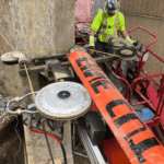
Slicing is done with a silicon wafer cutting wire sawa long loop of thin steel wire coated with bonded diamond abrasive that saws through the ingot. According to a 2025 review of wafer slicing by researchers at the University of Strathclyde (Mechanical Systems and Signal Processing, 2025), diamond wire sawing has become the dominant wafer-slicing technology precisely because it delivers better surface quality and lower kerf loss than older slurry methods.
“Kerf” is the silicon turned to dust by the cut itself. Here’s the uncomfortable arithmetic: with ultra-fine diamond wire under 50 µm, kerf width can be held to roughly 60–80 µm, but when you’re slicing wafers only ~150 µm thick, the material lost to the cut can approach the thickness of the wafer you keep. On modern high-throughput lines, multiple wires cut an entire ingot at once; this multi-wire slicing approach is what makes wafer economics work at scale.
⚠️ The slicing-before-circuit trap
Because slicing happens before any lithography, its defects are invisible on a process flow chart yet permanent in the finished wafer. Thinner wafers and harder materials (silicon carbide, sapphire) make this step harder, not easier — which is why wafering equipment, not just lithography, is a real lever on yield. For a deeper look at the substrate itself, see our guide to silicon wafer material and how it is made.
Oxidation & Deposition: Building the Thin-Film Layers

With a polished wafer in hand, the front-end loop begins. Each cycle’s first job is to put down a thin film, the raw material that the next pattern will be carved into. Films are only nanometers to a few hundred nanometers thick, and the method depend on the material and the precision required.
- ✔Thermal oxidationgrows a silicon-dioxide insulating layer by heating the wafer in oxygen or steam. Because that oxide is grown from the silicon itself, it bonds extremely cleanly.
- ✔Chemical vapor deposition (CVD)reacts gases at the wafer surface to deposit films such as silicon nitride or polysilicon.
- ✔By contrast, physical vapor deposition (PVD / sputtering) knocks atoms off a target so they settle on the wafer, usually for metals.
- ✔Finally, atomic layer deposition (ALD) lays down one atomic layer at a time for the thinnest, most uniform films, used as devices shrink.
Why so many methods? Because the film’s job decides the technique. An insulator that must be pinhole-free, a metal that must fill a narrow trench, and a gate dielectric a few atoms thick each demand different physics, and each new layer must be deposited without disturbing the patterned layers already underneath. Epitaxy, a related step, grows a fresh single-crystal silicon layer aligned to the wafer beneath it when device performance demands a pristine starting surface.
Photolithography: Printing the Circuit Pattern

Photolithography is the defining step of semiconductor manufacturing, it determines how small the transistors can be, and it’s repeated for every one of the ~90 layers. First the wafer is coated with a light-sensitive film called photoresist, then exposed to ultraviolet light projected through a patterned mask, or photomask, mounted on a reticle. Where the light lands, the resist change chemistry, transferring the mask’s blueprint onto the wafer.
What is photolithography in semiconductor manufacturing?
It’s photographic patterning at nanometer scale. Exposure wavelength sets the resolution limit: deep ultraviolet (DUV) light at 365 nm and 193 nm handles older and mid-range nodes, while the very finest features are printed with extreme ultraviolet (EUV) light at just 13.5 nm, a wavelength so short it must be generated by vaporizing tin droplets with a laser and focused entirely with mirrors, because it would be absorbed by ordinary lenses. For each layer the loop run: coat resist → align → expose → develop → inspect, then hand the wafer to etch.
“An EUV lithography scanner weighs about as much as two Airbus A320s and costs in the neighborhood of $380 million. There is exactly one company in the world that makes them, which tells you everything about why advanced nodes are so concentrated.”
That concentration is the real story of lithography. Because the most advanced patterning depends on a single supplier (ASML) and a handful of resist and mask makers, photolithography is both the technical heart of the process and its biggest geopolitical chokepoint, a theme that show up again in search demand, where interest in “photolithography” and “EUV lithography” has been climbing.
Etching, Doping & Ion Implantation

Lithography only creates a stencil in the resist. Two steps turn that stencil into real circuitry. Etching removes material through the openings in the resist, cutting the pattern down into the film below. Dry (plasma) etching uses reactive gases for sharp, vertical sidewalls and is standard at advanced nodes; wet etching uses chemical baths for less critical layers. Its real challenge is selectivity, removing exactly the intended film without damaging the layers beneath, sometimes to within a few atomic layers.
Then comes doping, which gives silicon its switchable electrical behavior. Pure silicon is neither a good conductor nor a good insulator; by introducing controlled impurities, boron to make p-type regions, phosphorus or arsenic for n-type, engineers create the junctions that make a transistor switch. Today’s dominant method is ion implantation: dopant atoms are ionized, accelerated, and fired into the silicon to a precisely controlled depth and dose, after which a high-temperature anneal repairs the crystal and activates the dopants. Older diffusion furnaces are still used for some steps, but implantation gives the depth control that small geometries require.
💡 Why this matters: etch defines the shape of a device; doping defines its electrical function. A flawless pattern with the wrong dopant profile is a dead transistor — which is why these two steps are tuned together, layer by layer.
Metallization, Interconnects & CMP

Once the transistors exist, they’ve to be wired together, and on a modern chip that wiring is its own multi-story city. This back-end-of-line stage (still inside the wafer fab, not to be confused with back-end packaging) builds 10 or more stacked layers of metal interconnects, usually copper, separated by insulating dielectrics. Its dominant technique is the copper damascene process: trenches are etched, lined, filled with electroplated copper, and the excess is polished away.
That polishing stepchemical mechanical planarization (CMP)is the unsung hero of multilayer chips. After each metal layer, CMP grinds and chemically polishes the wafer flat again, because lithography can only focus on a perfectly level surface. Skip it, and the small depth-of-focus of an advanced scanner means the next layer simply won’t print. CMP is run after deposition and metal steps throughout the flow, sometimes dozens of times per wafer.
So a finished wafer is really two structures stacked together: the transistors at the bottom, and a dense web of copper interconnects above them carrying power and signals, all built without ever disturbing the layers below.
Wafer Test, Dicing, Assembly & Packaging

When the wafer leave the front-end fab, it holds hundreds or thousands of finished dies, but they aren’t yet chips. Back-end processing turns them into packaged, testable products through four moves: probe test, dicing, assembly, and final test.
- Wafer probe / electrical sort: every die is electrically tested on the wafer; failures are marked so only good dies move forward.
- Dicing: the wafer is cut into individual dies. Cutting is done by a diamond dicing saw, laser, or plasma, and, like ingot slicing, it’s a hard-and-brittle cutting problem where kerf, chipping and edge strength decide yield. Precision diamond wire and blade dicing are used where thin or fragile dies can’t tolerate chipping.
- Assembly / packaging: each good die is bonded to a substrate and connected to the outside world by wire bonding or flip-chip bumps, then encapsulated. Package styles range from BGA and QFN to wafer-level chip-scale packaging (WLCSP) and stacked 3D packages.
- Last comes final testingthe packaged chip is checked again across voltage and temperature before it ships.
For decades this back-end was treated as the “easy” half. That assumption is now outdated: advanced packaging, stacking and linking multiple dies in one package, has become a primary way to keep performance scaling as transistor shrinks slow down.
Inside the Fab: Cleanroom, Equipment & Cost

All of the front-end happens inside a cleanroom, because at these dimensions a single airborne particle can ruin a die. Fabs are classified under ISO 14644-1, the international cleanroom air-cleanliness standard, with critical lithography and etch areas held to roughly ISO Class 1–5 — meaning the air carries only a handful of sub-micron particles per cubic meter, thousands of times cleaner than a hospital operating room.
That environment, plus the machines inside it, is why fabs are among the most capital-intensive factories ever built.
$10–20B
Cost of a new leading-edge fab
~$380M
Price of a single advanced EUV scanner
24/7
Continuous operation to amortize capital
A new advanced fab routinely runs $10–20 billion, with the building and its ultra-clean utilities alone costing several billion before a single tool is installed. Tooling accounts for the rest: lithography scanners, etchers, deposition chambers, implanters and metrology, supplied by a short list of firms including ASML, Applied Materials, Lam Research and Tokyo Electron. This is the honest answer to a question millions of people search every monthwhy can’t more countries just build their own chips? That barrier isn’t secrecy; it’s the multi-billion-dollar entry ticket, the single-source EUV supply, and the years it take to reach high yield.
⚠️ Common misconception
More process steps do not automatically mean a “better” chip. Each added step is another chance to introduce a defect, so fabs fight constantly to keep yield high while complexity climbs. A leading-edge process is a balance between feature size and the realistic yield a fab can hold — not a race to add steps.
Industry Outlook 2026: EUV, Advanced Packaging & Reshoring

Semiconductor manufacturing isn’t standing still, and three forces are reshaping it right now.
Market direction. The global semiconductor market reached roughly US$796 billion in 2025, according to the European Parliament’s 2026 briefing on the Chips Act, driven by demand for data-center and AI silicon. The 2026 Deloitte semiconductor outlook projects continued strong sales alongside a sharper focus on supply-chain risk.
Technology evolution. Two shifts matter most. First, lithography keeps advancing toward High-NA EUV to push features still smaller. Second, and more disruptiveadvanced packaging is moving from afterthought to main event. A 2025 analysis from Georgetown’s Center for Security and Emerging Technology (CSET) argues that stacking and integrating multiple dies (heterogeneous and 3D packaging) is now central to performance and supply-chain security, not a back-end commodity. Demand for wide-bandgap materials is rising too, pulling wafer-cutting technology toward harder substrates such as silicon carbide (SiC) wafer cutting, sapphire wafer slicing, and high-throughput solar silicon cutting.
Policy and geography. Reshoring is the headline. The Semiconductor Industry Association projects about $2.3 trillion in industry capital spending across 2024–2032 (versus $720 billion in the prior decade) and expects US manufacturing capacity to roughly triple by 2032. Europe’s Chips Act 2.0 pushes in the same direction. One catch, documented across the industry, is that building a leading fab outside Asia can take longer and cost more, so the next few years are about closing that gap, not just announcing projects.
What to do with this: if you’re sourcing chips or planning equipment investment for 2026–2027, watch advanced-packaging capacity and wafer-substrate supply as closely as the headline node race, those are where the bottlenecks (and opportunities) are moving.
Frequently Asked Questions
Q: What are the steps in the semiconductor manufacturing process?
View Answer
Core steps run from wafer preparation (ingot growth and slicing), through film deposition and oxidation, photolithography, etching, doping by ion implantation, and metallization with CMP, then finish with wafer testing, dicing and packaging. Because the deposit–pattern–etch–dope loop repeats for roughly 90 layers, a finished chip can involve hundreds to over 1,000 individual process steps spread across three to four months of fabrication.
Q: How long does it take to manufacture a semiconductor chip?
View Answer
From blank wafer to finished die typically takes 3–4 months of continuous fabrication, because fabs process roughly one mask layer every 1–1.5 days and a leading-edge chip has around 90 layers. Back-end packaging and test add days more on top of that.
Q: What is the difference between a fab and a foundry?
View Answer
A “fab” is the physical wafer-fabrication plant. A “foundry” is a business model — a company that runs fabs to manufacture chips designed by fabless customers, rather than selling its own branded products.
Q: Why can’t the US produce chips like Taiwan?
View Answer
It is catching up, but the barriers are time and money rather than knowledge. A leading-edge fab costs $10–20 billion, depends on single-source EUV scanners, and needs years to reach high yield with a deep supplier and talent ecosystem. US CHIPS Act money is funding a major build-out — the Semiconductor Industry Association projects domestic capacity to roughly triple by 2032 — but replicating Taiwan’s clustered front-end ecosystem takes more than one factory.
Q: What materials are used to make semiconductors?
View Answer
Single-crystal silicon is the dominant wafer material, refined to better than 99.99% purity. Dopants such as boron, phosphorus and arsenic tune its conductivity; copper forms the interconnects; and films of silicon dioxide and silicon nitride act as insulators. Wide-bandgap materials like silicon carbide (SiC) and gallium nitride (GaN) are growing fast for power and high-frequency devices.
Q: Who are the top semiconductor manufacturers?
View Answer
In leading-edge logic foundry manufacturing, TSMC, Samsung and Intel are the principal players, with TSMC holding the largest share of advanced-node production. Equipment that makes their processes possible comes from a separate short list — ASML (lithography), Applied Materials, Lam Research and Tokyo Electron among them.
Cutting wafers from ingots — or dicing finished wafers?
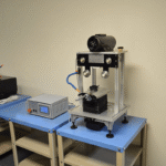
DONGHE builds diamond wire saws for the slicing and dicing of silicon, SiC, sapphire and other hard, brittle semiconductor substrates, engineered for low kerf loss and tight thickness control.
Why We Cover the Process Behind the Wafer
DONGHE builds diamond wire saws used in the ingot-slicing and wafer-dicing steps of this process, so we spend our days where kerf loss, total thickness variation and edge strength are decided. We wrote this guide to put those steps back into the full picture, because the wafer’s flatness budget is set by the cut long before the first transistor is ever printed.
References & Sources
- Semiconductor device fabricationWikipedia
- Competitive Semiconductor Manufacturing, cycle time per mask layerUC Berkeley IEOR
- Progress and Critical Challenges in Slicing of Thin Semiconductor Wafers (MSSP, 2025)University of Strathclyde
- ISO 14644-1 Cleanroom ClassificationInternational Organization for Standardization
- Re-Shoring Advanced Semiconductor PackagingCSET, Georgetown University
- America Projected to Triple Semiconductor Manufacturing Capacity by 2032Semiconductor Industry Association
- Chips Act 2.0, global semiconductor market briefing (2026)European Parliament (EPRS)
- 2026 Global Semiconductor Industry OutlookDeloitte
Related Articles & Resources
- Silicon wafer cutting wire sawingot slicing for low kerf loss
- Silicon wafer material: types, properties & how it’s made
- SiC wafer cutting sawslicing silicon carbide substrates
- Sapphire cutting wire saw
- Precision diamond wire sawfor thin and fragile materials
- Hard & brittle material cutting wire saw