Get in touch with DONGHE Company
-
Phone: +86 181-1645-5490
-
Email: Sales18@DongheScience.com

Aluminum Nitride (AlN) Substrate: Properties & Applications in Power Electronics
An aluminum nitride substrate is usually bought for thermal conductivity, electrical insulation, and dimensional stability. Cutting has to protect those values: low edge chipping, narrow kerf, controlled sub-surface damage, clean coolant handling, and enough process evidence for the next packaging or inspection step.
Use this guide when an AlN sheet, wafer, carrier, or ceramic substrate needs slicing, couponing, dicing, or sample preparation before a high-power electronics, LED, RF, GaN, IGBT, or thermal package build. Some drawings call the same material aluminium nitride; the cutting risks stay the same.
Quick Specs Card
Common workpieces
0.25-1.0 mm AlN sheets, thin ceramic substrates, test coupons, larger machined plates
0.25-1.0 mm AlN sheets, thin ceramic substrates, test coupons, larger machined plates
Starting wire speed
800-1200 m/min for AlN trial planning
800-1200 m/min for AlN trial planning
Starting feed range
0.1-0.3 mm/min, then adjust by chip size, Ra, and wire load
0.1-0.3 mm/min, then adjust by chip size, Ra, and wire load
Coolant default
Water-free or oil-based unless the substrate maker approves a water-based process
Water-free or oil-based unless the substrate maker approves a water-based process
Main inspection points
Kerf, Ra, edge chips, sub-surface cracks, bow, residue, and dimensional drift
Kerf, Ra, edge chips, sub-surface cracks, bow, residue, and dimensional drift
Best fit
High-value brittle ceramic cutting where scrap cost matters more than raw cut speed
High-value brittle ceramic cutting where scrap cost matters more than raw cut speed
Why Aluminum Nitride Substrate Cutting Needs a Different Process Window
 Substrate: Properties & Applications in Power Electronics 1")
Aluminum nitride, also written aluminium nitride in some material specs, is not just another white ceramic plate. Its value comes from a rare mix of high thermal conductivity, electrical insulation, low thermal expansion, and service in power electronics where heat must leave a chip or power module without creating an electrical path.
Reference data for AlN show why buyers care. Ioffe Institute’s NSM Archive lists a maximal measured thermal conductivity at 300 K of 2.85 W cm-1 K-1, equal to 285 W/(m K), and thermal expansion coefficients of 5.27 x 10⁻⁶ K-1 along the c axis and 4.15 x 10⁻⁶ K-1 along the a axis over 20-800 deg C. Those figures explain why AlN substrates are used where heat, insulation, and expansion matching all matter.
Bulk aluminium nitride data is useful, yet each component still carries its own density, grain quality, and processing history. Matching the cutting technology to those details helps protect the real part, not just the material name on a drawing.
Material-property handoff before cutting
Ask the substrate manufacturer for material properties, sizes and thicknesses, density range, and whether the piece is bulk aluminum nitride, a metallized plate, or another AlN ceramic form. Bulk AlN substrates are not judged by one thermal number alone; wurtzite structure, crystal quality, insulating properties, oxidation history, and circuit cleaning can all affect release.
In a PCB, power module, or high power package, the part has to insulate while helping the assembly cool. Do not turn a phrase such as “extremely high thermal conductivity” into an acceptance criterion unless the grade, test method, and functional electronics applications are clear before manufacturing teams integrate the part.
That ceramic property package leaves little room for rough handling during cutting. Small edge chips can become stress raisers. Hidden cracks may show up later during metallization, bonding, thermal cycling, or module assembly. Residue from the wrong coolant can also become a cleaning and reliability issue.
Because of that, the practical goal is not simply to cut through the material. Define a process window that protects the usable area of the substrate, keeps the kerf predictable, and gives quality teams enough evidence to release the part.
The AlN Damage Modes That Matter: Chipping, Sub-Surface Damage, and Coolant Risk
 Substrate: Properties & Applications in Power Electronics 2")
Visible damage often starts as edge chipping. It usually appears at the entry edge, exit edge, or unsupported corners. It is easy to see, easy to measure, and often the first reason a high-value part is rejected.
Harder to catch is sub-surface damage. Brittle ceramics can remove material through fracture, micro-crack growth, local ductile zones, and amorphized layers near the cut face. At low magnification, a surface may look acceptable while the near-surface region still carries damage.
Engineering Note
A 2026 Diamond and Related Materials abstract on diamond wire sawing of AlN reports a stable micro-amplitude oscillation window at 25-35 Hz and surface-quality degradation above 40 Hz. It also reports that lateral wire oscillation reduced the brittle-transition critical pressure from 2039.58 bar to 1129.32 bar while increasing amorphization and damage depth. In practice, more aggressive wire motion may remove material faster, but the cut face can pay for it.
Chemical and cleaning risk is the third damage mode. AlN is often discussed as a high thermal conductivity ceramic, but coolant chemistry cannot be treated casually. Some processes that are acceptable for alumina or zirconia may be a poor first choice for AlN substrates.
In 2023, Journal of Advanced Ceramics reported that raw AlN powder reacts easily with water to form Al(OH)3 or AlOOH. Finished substrates vary by purity, sintering aid, surface condition, and supplier, so the safest article-level rule is narrower: do not approve a water-based cutting process for AlN without supplier clearance, cleaning validation, and a sample-cut inspection record.
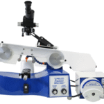
Diamond Wire Saw Parameters for Aluminum Nitride Substrates
 Substrate: Properties & Applications in Power Electronics 3")
Diamond wire sawing is a strong fit for thin AlN substrates because it can keep cutting force low while using a narrow abrasive path. It also supports controlled wet cutting, steady feed, and repeatable wire tension when the machine is built for brittle ceramics.
In DONGHE ceramic wire saw selection, the AlN starting point is 800-1200 m/min wire speed, 0.1-0.3 mm/min feed, and oil-based coolant. Treat those figures as trial-window inputs, not universal release specs. Thickness, substrate size, metallization status, desired Ra, and maximum edge chip allowance still decide the final setup.
| Parameter | Starting point | What to watch |
|---|---|---|
| Wire speed | 800-1200 m/min | Wire stability, vibration marks, cut face temperature, edge chip growth |
| Feed rate | 0.1-0.3 mm/min | Ra, wire loading, bow, corner break-out, exit-side chipping |
| Wire diameter | Match to kerf and stiffness target | Kerf loss, wire deflection, abrasive exposure, tension margin |
| Abrasive grit | Fine enough for Ra target; open enough to clear swarf | Surface scratches, wire loading, cut time, local heating |
| Coolant | Oil-based or other water-free system first | Residue, cleaning route, AlN-water compatibility, downstream bonding |
If the project involves very thin nitride substrates, metallized AlN, or a tight cosmetic edge requirement, run the first coupon as a documented sample cut. Record wire, feed, coolant, fixture contact, kerf, Ra, chip size, and microscope images before releasing the next batch.
Coolant and Fixturing Rules for AlN: The Oil-Coolant Decision Gate
 Substrate: Properties & Applications in Power Electronics 4")
Coolant selection for AlN is a decision gate, not a small machine setting. It affects heat removal, swarf flushing, chemical exposure, cleaning, and later assembly. Start with a water-free coolant when no supplier-approved water route exists.
Use oil-based coolant first when
- The substrate supplier has not cleared water exposure.
- If the part will be bonded, metallized, or cleaned under a strict residue spec.
- When the cut face must meet a tight Ra or edge-chip target.
- If the AlN grade, sintering aid, or surface treatment is unknown.
Consider another coolant only when
- The material maker approves the chemistry.
- Coupon cutting passes microscopy, cleaning, and electrical checks.
- Drying and storage rules are written before production.
- Residue tests show no bonding or thermal-interface issue.
Fixturing is the second gate. AlN substrates are often thin enough that clamping pressure can create bow or hidden stress. Use broad support, soft contact surfaces, and a sacrificial backing when exit-side chip control matters. Do not leave long overhangs near the final cut.
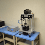
When selecting a machine, compare a production endless loop system with a smaller laboratory diamond wire saw. During first coupon learning, a lab saw may fit better; an endless loop or CNC setup is better once the recipe is fixed.
AlN vs Alumina, Silicon Nitride, and Silicon Carbide Cutting Difficulty
 Substrate: Properties & Applications in Power Electronics 5")
AlN sits between familiar technical ceramics in a difficult way. It is not as hard as silicon carbide, but the substrate value, coolant concern, and thermal-package use case make scrap more expensive. This comparison is a cutting planning view, not a full material-property database.
| Material | Typical driver | Cutting concern | Planning note |
|---|---|---|---|
| AlN | Heat spreading plus insulation in power electronics | Coolant compatibility, edge chip, sub-surface damage | Document coolant and inspection before scaling |
| Alumina | Cost-effective ceramic substrates and wear parts | Brittleness and edge chipping | A common baseline for ceramic diamond wire saw trials |
| Silicon nitride | Strength, bearings, wear, thermal-shock service | Toughness and slower removal | Feed and wire loading need close control |
| Silicon carbide | High-power semiconductor and wear applications | Hardness, wire wear, micro-cracking | See SiC wafer cutting saw planning for harder wafers |
Demand for AlN keeps getting stronger because of thermal performance. ACS Nano reported low-temperature sputtered AlN thin films from 100 nm to 1.7 um and showed about a 3x change in thermal conductivity for about 600 nm films as process conditions changed. Cutting buyers should take one lesson from that sensitivity: rough cutting should not be allowed to become the weak step in the chain.
The 7-Parameter AlN Cutting Risk Matrix
 Substrate: Properties & Applications in Power Electronics 6")
Score the job below before asking for a quote. This matrix turns a vague “can you cut AlN?” request into an RFQ that engineering, quality, and purchasing can all read.
| Risk parameter | Low-risk input | Higher-risk input | What to send with the RFQ |
|---|---|---|---|
| 1. Thickness | 0.5-1.0 mm plate | Very thin sheet below 0.38 mm or thick block | Nominal thickness and tolerance |
| 2. Outline size | Small coupons with full support | Large panels or long unsupported strips | Drawing, cut length, and support limits |
| 3. Surface finish | Ra target used for fit only | Ra tied to bonding, sealing, or metallization | Ra/Rz target and measuring method |
| 4. Edge chip allowance | Cosmetic allowance wider than 50 um | Active area near the cut edge | Max chip size and inspection magnification |
| 5. Coolant restriction | Oil-based allowed | Water, residue, or cleaning restrictions unclear | Approved coolant list and post-cleaning spec |
| 6. Metallization status | Bare substrate | DBC, AMB, thick film, or plated features nearby | Layer stack, keep-out zone, and cleaning limit |
| 7. Acceptance proof | Visual and dimension check | Microscopy, thermal, electrical, or bonding release | Inspection plan and pass/fail limits |
| 8. Batch value | Low-cost trial material | Expensive AlN substrates or short lead-time inventory | Scrap cost and sample allowance |
| 9. Throughput target | Prototype or R&D pieces | Repeat lots with cycle-time pressure | Monthly quantity and takt target |
If three or more columns land in the higher-risk side, request a sample-cut process window before buying fixtures, wire inventory, or full production equipment.
How to Inspect Cut Quality After AlN Substrate Sawing
 Substrate: Properties & Applications in Power Electronics 7")
Inspection should match the failure mode. Checking dimensions alone is not enough for a heat-spreading ceramic that may go into a power device or electronic package.
- Confirm kerf and dimension by checking cut width, final length, and tolerance stack from the drawing.
- Inspect edge chip size on both entry and exit edges at the magnification named in the spec.
- Measure surface roughness, including Ra and, when needed, Rz across the cut face.
- Use sub-surface crack checks such as microscopy, dye, cross-section, or another agreed method for high-risk parts.
- Check bow and flatness on thin AlN sheets after unclamping and after cleaning.
- Verify residue removal before bonding, metallization, or thermal-interface assembly.
- Record traceability details: wire batch, feed, speed, coolant, and fixture condition.
Adjacent brittle ceramic research supports this inspection-first mindset. In a 2024 Materials paper, researchers cut polycrystalline SiC with a diamond wire saw and used SEM, laser confocal microscopy, FIB, and TEM to connect feed rate, surface roughness, ductile zones, brittle fracture, and amorphization. AlN is not SiC, but the measurement logic transfers well: if the application is high value, inspect more than the outside edge.
Inspection Standards and RFQ Scenarios for AlN Cutting
 Substrate: Properties & Applications in Power Electronics 8")
Standards are not cutting recipes, but they make acceptance language less vague. If the drawing references flexural strength, point the buyer to ASTM C1161 or ISO 14704. If crack tolerance or fracture behavior is part of release, use ASTM C1421 or ISO 18756 as the test-language reference. For hardness and density language, cite ASTM C1327 and ASTM C373 where they fit the material and buyer requirement.
A practical RFQ can name the inspection method without pretending the cutting supplier controls the original ceramic grade. Use ASTM or ISO language for the property test, then name the cutting acceptance limit: kerf 150-250 um, edge chip below 50 um, Ra 0.3-0.6 um, thickness drift below 0.02 mm, and no visible cracks at the agreed magnification. The NISTIR 5030 reference is useful when an engineering team wants a neutral material-property trail rather than a supplier catalog.
For release planning, add the inspection setup to the RFQ rather than leaving it for the first production lot. A practical note can specify a 2 mm sacrificial backing strip, fixture overhang below 5 mm near the exit edge, a 24 hour post-cleaning hold before final review, and storage below 40% relative humidity when the material supplier flags moisture sensitivity.
Scenario 1: 20-piece R&D coupon project
Baseline: a lab needs 20 coupons from 0.5 mm AlN sheet in 10 business days. Set reject rate tracking before cutting: edge chips above 50 um count as rejects, and any coolant residue after cleaning is a rework item. The production outcome to watch is not raw throughput; it is how many coupons survive microscope review without rework.
Scenario 2: metallized power-module substrate
Baseline: a 0.635 mm metallized plate needs a 114 mm cut length near active circuit area. The project timeline should include one sample cut, one cleaning review, and one edge inspection before release. Track rework rate by cause: chipping, bow, residue, or dimensional drift.
Scenario 3: 1,000-piece monthly deployment
Baseline: a buyer moves from prototype to 1,000 pieces per month and needs predictable throughput. Compare 300-500 um blade kerf against a 150-250 um diamond wire kerf, then track scrap cost, wire change interval, and inspection time per lot. A deployment plan should freeze the coolant, fixture, wire lot, feed, and speed before volume release.
Diamond Wire Sawing vs Blade, Laser, and Waterjet for AlN Substrates
 Substrate: Properties & Applications in Power Electronics 9")
AlN cutting method selection depends on thickness, heat sensitivity, edge quality, coolant rules, and production volume. Each method has a practical tradeoff.
| Method | Advantages | Limitations for AlN | Best use |
|---|---|---|---|
| Diamond wire saw | Low force, narrow kerf, good for brittle ceramic substrates | Needs wire, coolant, tension, and feed recipe control | Precision AlN coupons, wafers, sheets, and thermal substrate cutting |
| Diamond blade saw | Familiar shop process and direct setup | Higher force and wider kerf can raise edge-chip and scrap risk | Lower-value or thicker parts with wider tolerance |
| Laser cutting | No mechanical contact and fine path control | Heat-affected zone, recast, and thermal cracking risk must be checked | Thin features when heat effects are acceptable |
| Waterjet | Low thermal load and flexible shapes | Water exposure, abrasive embedding, wider kerf, rougher edge | Non-electronic ceramic blanks when chemistry and edge finish are acceptable |
For equipment routing, start with precision diamond wire saw options, then compare multi-wire saw machine types if batch slicing is the real bottleneck.
Send a Better AlN Cutting RFQ
A useful RFQ for AlN substrates has more than size and quantity. Include the material grade, thickness, cut length, allowed kerf, desired Ra, edge-chip limit, coolant restrictions, cleaning requirement, inspection method, and monthly volume.
To have DONGHE review the cut, route ceramic projects through the ceramic diamond wire saw page and request either an AlN sample-cut process window or a machine selection review.
2026 Outlook: Lower-Damage Wire Sawing for High-Power AlN Applications
 Substrate: Properties & Applications in Power Electronics 10")
AlN substrates are moving with high-power, high-frequency, and wide bandgap electronics demand. GaN devices, RF modules, LEDs, optoelectronics, and dense power modules all reward better heat paths. That keeps pressure on cutting, because a high thermal conductivity substrate still fails the business case if too many parts are lost to chips, cracks, or residue.
Long-running reference collections such as NISTIR 5030 show that the property side is mature enough to track AlN across mechanical, electrical, and thermal datasets. Direct process-control evidence for cutting is still growing, including the 2026 AlN diamond wire sawing study.
Near-term work points to better wire motion control, better fixturing, cleaner coolant rules, and inspection plans that measure the damage mode the part actually cares about. Related high-tech cuts include DONGHE pages on silicon wafer cutting, sapphire cutting, and the broader high-tech precision equipment category.
FAQ
Can aluminum nitride substrates be cut with a diamond wire saw?
Yes, when the saw can hold stable wire tension, slow feed, controlled coolant delivery, and support near the cut line.
What coolant should be used for AlN cutting?
Use an oil-based or other water-free coolant as the starting point unless the substrate supplier and your sample-cut data approve a water-based route. AlN-water behavior depends on material form, sintering aid, and surface condition. Run a cleaning check as well as a cut-quality check before production approval.
What wire speed is a reasonable first test for AlN?
DONGHE ceramic wire saw planning uses 800-1200 m/min as a starting range paired with a 0.1-0.3 mm/min feed test. Final values depend on thickness, target Ra, wire diameter, abrasive grit, coolant, fixture support, and chip allowance.
Is laser cutting better than wire sawing for AlN?
Laser cutting may be useful for thin features, but heat effects, recast, and thermal cracks must be checked. Where kerf, edge quality, and low mechanical stress all matter, diamond wire sawing is often the safer first process to test. Ask for microscope images of the cut face before assuming a contact-free method gives a lower-damage result.
What should be included in an AlN substrate cutting RFQ?
Send the grade, drawing, thickness, cut length, kerf target, Ra target, chip limit, coolant rules, cleaning requirement, inspection method, quantity, and whether the part is bare, metallized, or bonded.
References & Sources
- Ioffe Institute NSM Archive: Aluminium Nitride thermal properties
- NISTIR 5030: Cryogenic properties of inorganic insulation materials for ITER magnets
- ACS Nano: High Thermal Conductivity of Submicrometer Aluminum Nitride Thin Films
- Journal of Advanced Ceramics: Anti-hydrolysis modification of AlN powder
- Diamond and Related Materials: Surface damage mechanism and process control in diamond wire sawing of aluminum nitride
- Materials 2024: Material Removal Mechanisms of Polycrystalline Silicon Carbide Ceramic Cut by a Diamond Wire Saw
- ASTM C1161: Flexural strength of advanced ceramics at ambient temperature
- ASTM C1421: Fracture toughness of advanced ceramics at ambient temperature
- ISO 14704: Flexural strength of monolithic fine ceramics at room temperature
- ISO 18756: Fracture toughness of monolithic ceramic materials