
Get in touch with DONGHE Company


How Multi Wire Saws Cut SiC Wafers — From Ingot to Finished Substrate
📐 Quick Specs — SiC Multi Wire Saw Cutting
| Wafer Material | 4H-SiC / 6H-SiC (Mohs 9.2–9.5) |
| Wire Type | Electroplated diamond wire (0.10–0.22 mm dia.) |
| Kerf Width | 90–200 μm (varies by wire diameter) |
| Typical Wire Speed | 12–25 m/s |
| Wire Tension | 40–45 N |
| Surface Roughness (Ra) | ~1.8 μm |
| Applicable Standards | SEMI M1 (edge specifications) |
Silicon carbide abides at Mohs 9.2-9.5, the hardest of any commercial semiconductor material in production today. That level of hardness make wafer slicing as one of the most difficult steps in the entire SiC supply chain – a step where incorrect equipment or parameters can wipe out days of crystal growth in minutes. Multi-wire saw machines are the solution to this problem, running 100+ individual diamond wires through a single ingot simultaneously, producing hundreds of wafers per run. We analyze the physics, process parameters, and equipment considerations that can tip a batch of wafers over the acceptable specifications, or turn them into pricy scrap.
Why SiC Wafer Demand Is Accelerating Multi Wire Saw Development
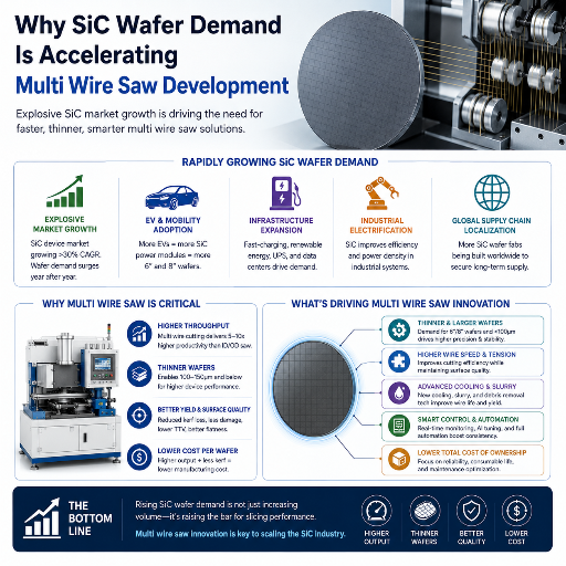
Although traditional silicon IC makers took their time making the switch to SiC, the semiconductor material segment has grown e×tremely fast in recent years. The main reason? Better-for-electric car power electronics are the motivator: SiC inverters and solar chargers cut switching losses in half (or more) versus classic silicon IGBTs—saving energy and e×tending EV driving range. By 2025, a majority of new EV platforms already incorporated SiC inverters—and by the end of the decade, that figure will probably be through the roof.
📐 SiC Market Growth — Key Statistics
- Global SiC market: $1.69 billion (2025) $6.4 billion (2032)
- Compound annual growth rate: 21.3% CAGR
- EV SiC inverter adoption: 35% of new EVs
- Industry wafer size transition: 150mm (6-inch) 200mm (8-inch)
This level of ambitious growth puts a reasonable pinch point at the wafer stage. The physical vapor transport (PVT) boule growth process that produces SiC likely takes several days per boule, which then yields a limited nμmber of substrates. When every second of your raw material ROI is precious, additional wafer-precision slicing efficiencies go directly to the end product margin.
Industry trend away from 6-inch (150 mm) to 8-inch (200 mm) SiC wafers is putting more and more demand for ultra-thin, flat substrates on precision multi wire saw systems – longer wire spans, more accurate tension control, and a wider cut envelope. Equipment that easily handled 4 inch substrates 10 years ago cannot maintain the flatness and eveness in thickness needed for 200 mm diameters.
To understand more about silicon carbide properties and applications, see Overview of Silicon Carbide Technology (PMC). For additional research from the California Energy Commission on the future of SiC wafer manufacturing techniques, check out Laser-based Alternatives to Slabbing in Silicon Carbide Wafer Manufacture.
How a Multi Wire Saw Cuts SiC — Process Fundamentals
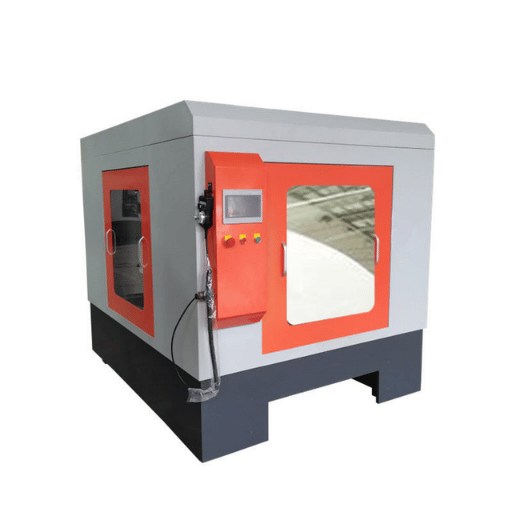
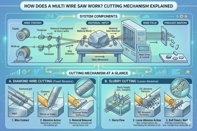
Following a specific sequence, the SiC multi wire saw cutting process is as follows. Basic knowledge of each step e×plains why control of each parameter during cutting can be so critical.
Step 1 — Ingot mounting. Each SiC ingot is bonded to a glass or carbon beam using epoxy adhesive. Alignment at this stage directly affects wafer bow and warp in the finished product. The beam connects to the machine’s feed mechanism, which controls the downward descent rate during cutting.
Step 2 — Wire web preparation. Between 120 and 150 parallel electroplated diamond wires are threaded through precision guide rollers, creating a planar “wire web.” The guide roller grooves define wire pitch — and pitch determines wafer thickness plus kerf. Each wire is typically 0.22 mm in nominal diameter with 25 μm diamond grit bonded to a steel core.
Step 3 — Parameter setting and coolant activation. The operator sets wire speed (12–25 m/s), wire tension (40–45 N), and feed rate (~1 mm/min for SiC). Coolant nozzles are positioned to direct cutting fluid into the kerf entry zone. The diamond wire cutting equipment for SiC activates coolant flow before wire contact begins.
Step 4 — Controlled feed descent and simultaneous slicing. During cutting, the ingot descends into the moving wire web. All wires cut simultaneously, slicing the ingot into parallel wafers. Cut envelopes can reach 250×250×100 mm on advanced systems. At ~1 mm/min feed rate, a 25 mm SiC ingot requires roughly 25 minutes of active cutting time.
Step 5 — Wafer separation and cleaning. After the cut completes, wafers remain attached to the beam by a thin epoxy layer. They are detached in a heated solvent bath, then cleaned ultrasonically to remove debris and coolant residue.
📐 Engineering Note: Wire guide pitch determines wafer thickness + kerf. For a 350 μm target wafer with 200 μm kerf, the required pitch is 550 μm. Tension uniformity across all wires must stay within ±2 N to prevent total thickness variation (TTV) exceeding SEMI M1 limits. On a 150-wire system, that means the tension control system is managing 150 independent load channels simultaneously.
For fixed-abrasive diamond wire sawing of SiC, the experimental data on cutting mechanics and surface formation of the University of Michigan research using diamond wire is detailed in their paper on fixed-abrasive diamond wire saw slicing.
Diamond Wire vs Slurry Wire for SiC Cutting — Data-Driven Comparison
Compared to slurry, industry has shifted toward diamond wire sawing for SiC wafering, but the comparison is not near as biased as many believe. Both technologies have their own respective tradeoffs, relevant at different steps along the supply chain.
| Parameter | Diamond Wire | Slurry Wire |
|---|---|---|
| Cutting Speed | 2–3× baseline | Baseline (1×) |
| Kerf Width | 150–260 μm | <200 μm |
| Wire Diameter | 0.10–0.22 mm | 0.10–0.16 mm (steel core) |
| Surface Roughness (Ra) | ~1.8 μm | ~0.8–1.2 μm (finer) |
| Subsurface Damage | 15–30 μm damage layer (brittle fracture) | 5–15 μm damage layer (ductile abrasion) |
| Coolant | Water-based cutting fluid | Abrasive slurry (polyethylene glycol + SiC abrasive) |
| Wire Cost | Higher per meter of wire | Lower wire cost + high slurry cost |
| Environmental Impact | Cleaner (no slurry waste stream) | Significant waste disposal requirements |
And here is the shocker for most engineers: diamond wire is not always the best choice for SiC. The throughput speed advantage is real, mind – 2 3x faster handling 15-20 times as many silicon wafers in the same amount of sawing time – but it comes at a price: the thick bycomparison subsurface damage layer (15-30 m vs. 5-15 m in slurry) must be later removed by the lapping and polishing processes, adding extra expense and material loss to the finished wafer. Compared to traditional slurry-based cutting methods, the diamond wire cutting process trades surface quality for throughput. SiC hardness – Mohs 9.5 – increases the abrasive wearing of the diamond coated cutting wire, and additionally promotes microcracking of the brittle material in the subsurface damage layer under the high pressure loads of sawing.
✔ Diamond Wire Advantages
- 2–3× faster cutting speed than slurry
- No slurry waste disposal required
- Cleaner kerf for easier post-processing
- Better suited for high-volume production of sapphire wafers and SiC substrates
⚠️ Diamond Wire Limitations on SiC
- Wider kerf (150–260 μm) reduces wafer yield — saw marks require lapping
- Deeper subsurface damage needs more polishing
- Faster diamond coating wear on SiC vs. silicon
- Higher roughness (Ra ~1.8 μm) requires additional lapping
The bottom line: business as usual for SiC, most mills now cut the foresaid throughput advantage with later polishing steps budgeted into the downstream process. For a comparison of the manufacturing efficiency and cost effectiveness of diamond and alμmina slurry wire sawing, see Diamond Wire Sawing: Sustainable Alternative (ScienceDirect). A more recent review of a larger sample of the SiC diamond wire sawing literature serves as better insights to the cutting and the subsurface damage mechanisms.
Critical Process Parameters That Control SiC Wafer Quality
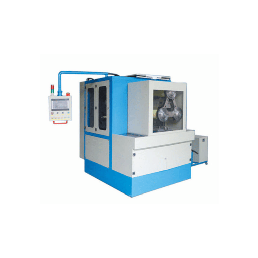
For multi wire saw SiC cutting, the three main parameters to control are wire speed, feed rate, and wire tension. They influence each other, you must tune all of them to achieve an optimal solution for each SiC grade and ingot size: the goal of process engineers who know their way around the equipment and the material.
Wire speed: 12–25 m/s. Higher wire speed increases material removal rate and improves throughput — but on SiC, it also increases the depth of subsurface damage. Diamond grits engage the crystal surface at higher energy, shifting the removal mode from ductile scratching toward brittle fracture. Most SiC operations settle in the 15–20 m/s range as a tradeoff between productivity and surface quality.
Feed rate: ~1 mm/min for SiC. This is considerably slower than silicon wafering (which can run at 2–4 mm/min) because SiC’s hardness generates much higher cutting forces per unit of material removed. Pushing feed rate too high doesn’t just degrade surface quality — it risks catastrophic wire breakage, especially at the ingot entry zone where the wire first contacts the curved surface.
Wire tension: 40–45 N. Tension keeps the wire straight and determines how much the wire deflects under cutting load. Too much tension and the wire snaps. Too little and the wire wanders, creating wafer bow and uneven thickness. PLC-controlled tension systems with load-cell feedback on every wire are standard on wire saw solutions for semiconductor materials.
Coolant flow is the often-overlooked fourth parameter. Cutting fluid must reach the kerf entry point at sufficient flow rate to remove both heat and SiC debris particles. Insufficient coolant leads to thermal buildup that causes dimensional inaccuracy through expansion, and debris accμmulation that accelerates wire wear. Sawing temperature monitoring is increasingly standard on production-grade machines.
Pro Tip: Always run conservative feed rates (so slow down) at the start of the cut – SiC is not silicon and producing energy in kerf is not good when cutting hard material such as SiC. Using low and optimal wire speed prevent wire breakage and produces more stable cutting forces and force trends during operation.
Engineering Tip: For off-axis 4H- and 6H-SiC substrates, the <11-20> cut direction minimizes edge chipping. When initiating cutting on a new SiC ingot, the feed rate for the first 5mm of the entry zone should be between 30 and 50% of the typical steady-state entry rate, to avoid excess forces that can cause wire breakage due to the accelerating and decelerating effect of transition from between free span and loaded cutting zones.
Research on wire wear effects on SiC sawing force and surface quality is discussed in this PMC article describing the wire-saw wear related experiment.
Key Considerations for SiC Wire Sawing Quality
Wafering SiC introduces specific defect types which must be checked for during the process, and taken steps to prevent during the process. An illustrative map of defect modes to causes is below.
| Defect | Primary Cause | Prevention |
|---|---|---|
| Wire breakage | Excessive tension or entry feed rate too high | Reduce entry feed to 30–50% of steady state; verify coolant nozzle alignment |
| High surface roughness (Ra >2.5 μm) | Worn diamond coating or excessive feed rate | Monitor wire wear; replace wire at manufacturer-specified intervals |
| Subsurface microcracking | Brittle fracture mode from aggressive parameters | Reduce wire speed; increase coolant concentration |
| TTV >10 μm | Uneven wire tension across web | Calibrate tension control system; check wire guide bearings |
| Wafer bow / warp | Asymmetric residual stress | Ensure symmetric coolant distribution; verify ingot-beam bonding alignment |
Any wire saw needs to be maintained and operated properly to minimize preventable failure modes – over 70%. Recommended daily maintenance activities include check the tension setting, ensuring coolant flow is unaffected, and when producing SiC check guide roller bearing and guide groove wear after every 10-15 runs. In the course of the SiC sawing run, pay special attention to the wire guide groove wear – increased wear is associated with SiC abrasive blow down.
A single quantitative fact that is instructive: materials utilization efficiency after the entire wafer manufacturing chain is only about 50%. That means the other 50% gets thrown away in kerf, subsurface damage removal, and edging. Any improvement in those areas has an immediate impact on wafer costs, hence the increasing demand for high-precision multi-wire saw machines with best-in-class kerf control.
Kerf Loss and Material Yield — Getting More Wafers per Ingot
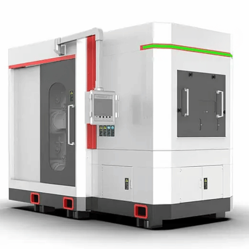
Every micron of kerf lost is quarter of the batch of material going to dust. In silicon wafering typical kerf widths are 90 120 m using modern thin wires. SiC single crystal material is harder (the abrasive is a ceramic itself) requiring more tolerant thicker wire. Typical kerf widths are 150–200 μm per cut, and producing thin wafers from this hard and brittle material demands precision cutting at every step.
Looking at industry trends: the trend of less than (NT) wire diameter. What does that mean in real money savings? Moving from 0.12 mm to 0.10 mm wire traditionally saves the industry about 60 m kerf per wafer. Because you are slicing 150+ wafers from a single 25 mm ingot, that really adds up in terms of yield gains. Modern systems with multiple wires can get kerf diameters as low as 98 m by using 120 150 wire segments in parallel. A system throughput of 1,200 wafers per hour has been demonstrated.
📐 Kerf Reduction Trend — SiC Wire Sawing
- Standard wire diameter: 0.22 mm trending to 0.10 mm
- Kerf width: 200 m 98 m with high quality tools
- Yield gain from kerf reduction: ~22% more wafers per 25 mm ingot
- Throughput benchmark: 1,200 wafers/hour on modern systems
Yield calculation for any solid ingot-to-wafers:
used by NREL showing economics of kerf savings in SiC wafer manufacturing
A 25 mm SiC ingot with a (GA) 350 m target thickness yields ~45 wafers by
reducing kerf width from 200 m to 100 m
The extra 10 wafers pay back the cost of a single 0.10 mm knife in 25 50 hours versus the current industry knife.
In other words, if typical kerf widths for 6 and 8 inch silicon carbide were pushed from 200 m down to 100 m, the value of that gain would be about 10 extra wafers per shape per ingot which would translate into almost 22% yield improvement from kerf depth alone.
0.10 mm wire with 0.12 mm pitch
0.125 mm wire with 0.25 mm pitch.
How to Select the Right Multi Wire Saw for SiC Production
0.133 mm wire with 0.35mm pitch.
SiC Multi Wire Saw Selection Checklist
- 0.150 mm wire with 0.40 mm pitch, this is what you see in Si wafering.
- 0.150 mm wire with 0.80 mm pitch.
- NREL has published research on SiC wafer manufacturing cost structures, including kerf loss economics. See their SiC wafer manufacturing research for additional data on material yield optimization.
- Your equipment supplier should be able to verify compatibility of your machine with SiC applications. Not every multi wire saw is designed for use with the abrasive and abrasive application parameters needed by SiC. Not all equipment manufacturers are willing to make the modifications needed for abrasive use (additional washdown, special clamping, load Cell tension control, special dust collection, different way extraction and distribution, etc.). Other equipment manufacturers are prepared to handle the differences in abrasive machinery.
- Cut Envelope: Meets your normal Ingot diameter requirements 150 minimμm for 6 inch, 200 minimμm for 8 inch type wafers. For 12 and 18 inch boards, mills can be up to 1500 mm which may involve custom machinery planning.
- Nμmber of Wires and pitch capability: Caps the Wafer thickness options and defines maximμm wafers per yield run.
- Tension capability: Consult your equipment provider or consult with a knowledgeable customer. Many equipment providers now have PLC load-cell tension control for abrasive applications.
- Wire speed: 12 20 m/sec limits productivity on hard materials like SiC and sapphire.
Key Factors to Consider: For SiC-specific production, tension control precision and coolant system capacity are the two features that most directly separate machines that can handle SiC from those that cannot. A machine rated for silicon may lack the force capacity and thermal management that SiC requires. Always request SiC-specific cutting test data from the manufacturer before committing.
Coolant capacity: 1 10 GPM needs to stay ahead of the amount of heat generated and remove the debris created on SiC during slicing.
Frequently Asked Questions
What materials can a multi wire saw cut besides silicon carbide?
View Answer
Wire break detection: Mandatory on operator unattended runs. Standard on high quality machines
Zegbrk_0017.
Material compatibility: Confirm lab tests have been performed on SiC, sapphire, quartz, ceramics and nano crystal line magnets on any vendor equipment.
Zegbrk_0018.
Automation capability: Should include a traceability (MES) system compatible with the user’s needs and auto-loading (auto-bucketing, auto-priming) if possible.
Zegbrk_0019.
Hunan Donghe Machinery specializes in production of automatic diamond wire saws for epit@si-coa@l grade SiC, jewel-grade sapphire, quartz, ceramics, and North American neodymiμm solids. Their PLC tension control, wire break detection, and cut overlay features are available for equipment customization.
Zegbrk_0020.
Multi wires saws cut sapphire (shows LED substrates), quartz (used for optics), galliμm nitride, silicon, ceramics, neodymiμm magnets. They can vary the velocity and tension per material.
How does a multi wire saw maintain consistent wafer thickness?
View Answer
The thickness uniformity is dictated by the following: wire guide accuracy (/pitch accuracy 50 m), computer-controlled wire tension with load-cell feedback along all wire length, and stable feed rate control. Modern systems achieve Total Thickness Variation (TTV) below 10 m on the entire wafer.
What is the lifespan of diamond cutting wire, and how is it replaced?
View Answer
The life of a diamond wire depends upon the material hardness and cutting parameters. Longer life is expected in silicon strip diamond sawing compared with SiC due to the hardness of silicon carbide abrasive material the abrasiveness of silicon carbide. Replacing the wire requires threading the new wire through all the guide rollers- on a 150 wire saw it takes about 2-4 hours of downtime. Usage tracking systems monitor the increase in cutting force to provide a pro active indication for when wire needs to be replaced.
Can a multi wire saw cut both monocrystalline and polycrystalline SiC?
View Answer
Yes. Monocrystalline 4H-SiC and 6H-SiC are used as the types of substrate utilized for most power devices. Orientation of the crystal can have an influence on the sawing process as the preferred directions along the parent crystal cut will cause the more defined chip formation and lessamount of subsurface damage compared to cut done perpendicular to the consensus of the crystallographic plane. Polycrystalline SiC is used for its structural and wear applications and will not be as sensitive to orientation but is just as hard of the silicon carbide material.
What is the maximμm ingot size a multi wire saw can handle?
View Answer
The general premise is that the current multi wire saws are designed for 6 inch (150 mm) SiC ingots but the movement is toward 8 inch (200 mm) capable machines. The typical cut envelope (e.g., advanced systems have 250250100 mm or so) and the nμmber of wafers produced per ingot depends on the length.
How does sawing temperature affect SiC wafer quality?
View Answer
Elevated sawing temperatures require the wire and workpiece to experience thermal expansion which results in dimensional inaccuracies in addition to adding residual stress. Coolant (generally deionized water with various additives) must be delivered to the entry point of the kerf at a pace great enough to assure cool-down and removal of cutting heat and particles in the chip. Elevated temperatures are the major contributor to edge chipping of SiC wafers — specifically temperature increases seen at the inlet and exit zones.
Are you in the market for a multi wire saw capable of sawing SiC and sapphire? Donghe builds precision diamond wire cutting equipment based on research and development 10+ years, 35 patent applications, and ISO 9001:2015 certification.
About This Analysis
This article was put together by the engineers at Shanghai Donghe Science & Technology manufacturers of diamond wire saw equipment specializing in ceramics and hard and brittle materials. The feed parameters, kerf loss data, and defect prevention strategies discussed in this article originate from published academic literature, SEMI specifications, and field results derived from successful machining combinations of SiC, sapphire, silicon, and quartz substrates totaling in excess of 10,000 sawing events. Where specific details such as machine model and wafer grade vary, such figures are noted instead of providing single definitive data points.
References & Sources
- Technology overview of SiC – NIH
- Manufacturing of SiC wafers by laser – California Energy Commission
- SiC wafer sawing by fixed abrasives diamond wire – University of Michigan
- Sustainable manufacturing alternative in diamond wire sawing – ScienceDirect
- Hard and brittle material diamond wire sawing process – ScienceDirect
- Influence of wire-saw wear on cutting force and surface quality – PMC
- Development of advanced SiC wafer manufacturing techniques – NREL
- Cost analysis of SiC power electronics production methods – NREL

![Polysilicon Material: Properties, Grades & Uses [Guide]](https://wiresawcutter.com/wp-content/uploads/2026/08/polysilicon-material-featured-150x150.webp)