Get in touch with DONGHE Company
-
Phone: +86 181-1645-5490
-
Email: Sales18@DongheScience.com

Types of Semiconductor Wafers: Silicon, SiC, GaN, GaAs, InP Compared
Buying a semiconductor wafer is not only a material decision. Wafer material shapes the device path, the fabrication limits, the inspection plan, and the way the slice behaves under wire, lap, polish, and etch steps. Logic ICs, solar cells, RF amplifiers, and high-power modules can all start from a round wafer. They should not start from the same buying checklist.
This guide compares the main wafer types by material family, electrical spec, application fit, and cutting risk. It is written for engineers and buyers who need a clear first pass before asking a wafer supplier or a cutting-equipment team for help.
Quick Specs: What To Decide First
| Decision field | Common choices | Why it matters |
|---|---|---|
| Main wafer families | Silicon, SOI, III-V, SiC, GaN, sapphire, specialty substrates | Sets the device application and process risk. |
| Common diameters | 100 mm, 150 mm, 200 mm, 300 mm; 450mm wafers remain a standards/watch item | Affects fab tooling, handling, yield model, and slicing format. |
| Electrical fields | Carrier type, dopant, resistivity, orientation | Controls device behavior before patterning starts. |
| Geometry fields | Thickness, TTV, bow, warp, edge, flat, notch | Decides whether the wafer can enter the next process without rework. |
| Cutting sensitivity | Lower for standard silicon; higher for SiC, sapphire, GaAs, and InP | Changes wire choice, feed speed, support, coolant, and inspection depth. |
What Is a Semiconductor Wafer?

In this context, a semiconductor wafer is a thin, circular slice of semiconductor material used as the base for electronic devices and integrated circuits. Substrate means the base material. Die means one patterned device area cut from that wafer after fabrication. Chip means the packaged or finished device people usually see later.
In semiconductor industry language, wafers are used as the starting platform for semiconductor devices. Wafers are made when raw silicon is pulled from molten silicon to form wafers from a monocrystalline semiconductor ingot, then sliced into thin wafers for later work. Materials other than silicon may use different crystal growth, bonding, or epitaxy routes. A wafer must fit the fabrication process; wafer manufacturing prepares the blank, while wafer fabrication builds devices upon the wafer.
Most wafers begin as a single crystal ingot, then move through slicing, shaping, lapping, polishing, cleaning, and inspection before device fabrication. That early mechanical history matters. Even a flat-looking wafer can still carry subsurface damage, poor TTV, or edge chips that later show up during lithography, etch, bonding, or thinning.
If your question is mainly how silicon wafers are cut, the deeper process article is DONGHE’s silicon wafer cutting wire saw page. This guide starts one step earlier: which wafer material and spec package should you use?
The 10-Wafer Substrate Triage Map For Types Of Semiconductor Wafers

To compare different types of semiconductor wafers quickly, group them by substrate family first, then by purchase spec and process risk. Use this triage map as a first filter, not a final process recipe. Device design, fab line rules, and supplier availability still decide the final wafer.
Different wafers play different roles in a semiconductor project. Compound semiconductor wafers can solve RF, photonics, or power problems that standard crystalline silicon cannot, while large wafers such as 300mm wafers can change dies per wafer, carrier needs, and material-loss economics. Semiconductor wafer technology keeps moving, but the first decision is still practical: which wafers that can be used in your fab route can your supplier actually deliver?
| Wafer type | Material family | Common device fit | Specs to confirm | Cutting or process risk |
|---|---|---|---|---|
| Intrinsic silicon wafer | Single crystal silicon | Research, detectors, clean baseline studies | Diameter, orientation, resistivity, thickness, TTV | Moderate; purity and surface condition matter more than dopant type. |
| P-type silicon wafer | Boron-doped silicon | CMOS, MEMS, solar cell work, sensors | Dopant, resistivity in ohm-cm, orientation, flat/notch | Moderate; do not mix P+ and P- lots without checking resistivity. |
| N-type silicon wafer | Phosphorus, arsenic, or antimony doped silicon | Power devices, research devices, high-lifetime solar cells | Dopant, carrier type, resistivity, oxygen/carbon limits | Moderate; supplier certificate must match device assumptions. |
| Epitaxial silicon wafer | Silicon layer on silicon substrate | Analog, power, image sensor, high-control device layers | Epi thickness, epi resistivity, substrate spec, defects | Layer quality can matter more than bulk wafer cost. |
| SOI wafer | Silicon on insulator | RF, MEMS, high-speed CMOS, isolation-sensitive devices | Device layer, buried oxide, handle wafer, thickness uniformity | High if thinning, bonding, or stress control is weak. |
| SiC wafer | Wide-bandgap silicon carbide | EV inverters, power modules, harsh-environment electronics | Polytype, off-axis angle, micropipe/defect limits, thickness | High; hard, brittle, and expensive substrate. |
| GaN wafer or GaN-on-substrate | Wide-bandgap III-V | LEDs, RF, power devices, fast switching | Substrate type, epi stack, defect density, bow | High; lattice mismatch and film stress can dominate. |
| GaAs wafer | III-V compound semiconductor | RF, microwave, optoelectronics, LEDs | Orientation, dopant, mobility target, surface finish | High; fragile handling and thermal limits need care. |
| InP wafer | III-V compound semiconductor | Telecom lasers, photonics, infrared devices | Crystal orientation, dopant, thickness, edge quality | High; crack and surface-damage control deserve early review. |
| Sapphire wafer | Aluminum oxide substrate | LED substrates, optical windows, RF insulation | Orientation, thickness, surface finish, bow/warp | High; hard and brittle material with edge-chip risk. |
| Diamond or AlN wafer | Specialty substrate | Thermal, RF, high-power research, advanced packaging | Grade, size, thickness, thermal need, defect limits | Very high; treat as a custom process review. |
BYU’s substrate reference groups wafer substrates into silicon, SOI, III-V compounds, II-VI compounds, SiC, sapphire, and other semiconductor material classes. DOE’s wide-bandgap assessment also separates SiC and GaN from silicon because their high-voltage and high-temperature behavior changes power-electronics design.
What are the different types of wafers?
Common semiconductor wafer types include silicon wafers, doped P-type and N-type silicon wafers, epitaxial silicon wafers, SOI wafers, SiC wafers, GaN wafers, GaAs wafers, InP wafers, sapphire wafers, and specialty substrates such as diamond or AlN. Use case, not name alone, decides the useful category.
Types Of Silicon Wafers: Intrinsic, P-Type, N-Type, Epi, And SOI

Silicon wafer buying starts with crystal quality, orientation, dopant, and resistivity. Pure silicon with no intentional impurity is called intrinsic. Once you dope silicon with boron, phosphorus, arsenic, or antimony, it becomes an extrinsic semiconductor with P-type or N-type behavior.
Older textbooks often compare silicon or germanium, but high-quality silicon wafers dominate most modern RFQs. Silicon wafers are available in many grades, and different silicon lots can vary by diameter of wafers, orientation, resistivity, and finish. Crystallographic planes of the wafer matter because a flat or small notch to convey wafer orientation tells the fab how the silicon surface should be aligned. SOI wafers feature silicon over silicon dioxide, so the wafer contains both a device layer and an insulating layer.
| Silicon wafer type | What changes | Buyer check |
|---|---|---|
| Intrinsic silicon | No intentional dopant; close to pure silicon | Ask for crystal method, impurity limits, and resistivity range. |
| P-type silicon | Boron usually creates hole-dominant behavior | Match P+, P-, and ohm-cm value to the device plan. |
| N-type silicon | Phosphorus, arsenic, or antimony usually creates electron-dominant behavior | Confirm dopant, lifetime, resistivity, and orientation. |
| Epitaxial silicon | A controlled crystal layer is grown on a substrate | Separate substrate specs from epi-layer thickness and resistivity. |
| SOI | A buried insulator isolates a silicon device layer | Confirm device layer, buried oxide, handle wafer, and stress limits. |
SEMI M1-0924 covers ordering information and requirements for high-purity electronic-grade single crystal polished silicon wafers, including substrates for epitaxial, annealed, and SOI wafers. That is why a silicon wafer RFQ should not stop at diameter and price.
Silicon remains the default starting point for many electronics applications because the supply chain, fab equipment, inspection methods, and process recipes are mature. That does not make every silicon wafer equal. One 100 mm P-type test wafer, one 150 mm MEMS wafer, and one 300 mm epitaxial wafer can sit in different procurement lanes.
Wide-Bandgap Semiconductor Material: SiC, GaN, Sapphire, And Specialty Wafers

Wide-bandgap wafers come into the discussion when silicon cannot handle the voltage, temperature, frequency, or optical requirement. DOE identifies SiC and GaN as two major wide-bandgap materials for power electronics, with higher voltage and temperature limits than silicon.
| Material | Why buyers use it | Spec and handling warning |
|---|---|---|
| SiC | High-power and high-temperature devices; BYU lists an Eg of about 2.9-3.05 eV | Confirm polytype, offcut, defect limits, and cutting support early. |
| GaN | Blue LEDs, lasers, RF, and power devices; BYU lists an Eg around 3.5 eV | Substrate mismatch and epi stress can drive reject risk. |
| Sapphire | Optical, RF insulation, and LED substrate use | Hardness and brittleness raise edge-chip and surface-finish risk. |
| Diamond and AlN | Thermal and advanced high-power research paths | Treat as custom lots with process trials before scale-up. |
For cutting discussions, SiC and sapphire should be routed differently from standard silicon. DONGHE keeps separate pages for the SiC wafer cutting saw and the sapphire cutting wire saw because hard and brittle substrates need tighter process review than a simple “same saw, new material” assumption.
III-V And Photonics Wafers: GaAs, InP, GaN, And Related Materials

III-V wafers move the decision away from commodity silicon and toward device physics. GaAs is a direct-bandgap material with high electron mobility, which is why it appears in RF, microwave, and optoelectronic devices. BYU lists GaAs with an Eg of 1.43 eV and notes thermal instability above 600 C.
InP is common in photonics and telecom contexts where light generation or detection matters. GaN crosses both groups: it is a III-V material, and it is also a wide-bandgap power and LED material. That overlap is one reason “wafer type” alone is not enough. GaN-on-silicon, GaN-on-SiC, and bulk GaN do not ask for the same process assumptions.
Use III-V wafers when the device needs speed, RF performance, laser behavior, or optical response that silicon cannot provide. Then check fragility, surface finish, and thermal limits before sending the lot into slicing, polishing, bonding, or thinning. For readers comparing saw paths after material selection, DONGHE’s semiconductor multi wire saw article is a better next stop than a general wafer taxonomy page.
Wafer Thickness And Specs Buyers Should Confirm Before Ordering

A wafer supplier can only quote the right wafer if the RFQ has enough fields. “Silicon wafer, 150 mm” is not a spec. It is a starting point.
For one single wafer, the edge of the wafer can decide whether the next step starts cleanly or stalls at incoming inspection. The term substrate is used to denote the base on which layers or devices are built. Wafers also carry purchase-history clues: wafers grown for research, high-quality wafers for production, and wafers that meet a special flatness or wafer processing target should not be mixed in one lot.
| RFQ field | Example values | What it protects |
|---|---|---|
| Diameter | 100 mm, 150 mm, 200 mm, 300 mm | Fab carrier, handling, cassette, and saw format |
| Thickness | 525 um for 100 mm silicon; 675 um for 150 mm silicon in BYU examples | Mechanical strength, thinning allowance, and breakage risk |
| Orientation | <100>, <111>, or project-specific orientation | Etch behavior, device layout, and flat/notch marking |
| Dopant and carrier type | Boron P-type; phosphorus N-type | Electrical behavior and process compatibility |
| Resistivity | Low, medium, or high ohm-cm range | Device performance and lot matching |
| TTV, bow, warp | BYU examples include 10 um TTV and 40-60 um bow/warp limits | Lithography, bonding, polishing, and inspection yield |
| Surface finish | Etched, single-side polished, double-side polished | Particle control, roughness, and next process step |
| Edge and packaging | Chamfer, bevel, notch/flat, carrier, clean-room bagging | Cracks, chips, contamination, and shipping loss |
BYU’s wafer-spec reference lists diameter, thickness, orientation, dopant, resistivity, bow, warp, TTV, and surface finish as practical spec fields. Its glossary defines bow as centerline curvature, warp as non-planar deviation with concave and convex regions, and TTV as total thickness variation between measured points.
If the question includes upstream ingot preparation, add the crystal diameter, cropping allowance, target slice thickness, and kerf target before asking for equipment advice. DONGHE’s ingot cropping wire saw page fits that earlier step.
Which standards belong in a wafer cutting RFQ?
Keep wafer material standards separate from the shop-floor scenario. SEMI M1 handles polished single crystal silicon wafer ordering, while ISO 14644-1 helps define cleanroom air-cleanliness classes for handling and inspection areas. A cutting project should also name machine-safety context: OSHA 1910.212 and CFR Part 1910.212 cover general machine guarding, while NIOSH material guidance belongs in the review when fine particles or advanced materials are part of the work. ISO, OSHA, CFR Part 1910, and NIOSH do not replace SEMI wafer specs; they frame the environment around wafer processing. Put that standards list beside physical lot fields such as 100 mm, 150 mm, 200 mm, or 300 mm diameter and any under-1 mm handling limit.
How thin are semiconductor wafers?
Many finished wafers are under 1 mm thick, but the right thickness depends on diameter, material, device route, and later thinning. BYU gives silicon examples of 525 um for 100 mm wafers and 675 um for 150 mm wafers. Thin wafers can reduce material use, but they also raise breakage and handling risk.
How Wafer Type Changes Slicing, Wafer Surface Risk, And Fabrication

Electrical purchasing checks do not guarantee a clean mechanical process. Cutting creates a surface. That surface then goes into lapping, polishing, cleaning, etch, bonding, or fabrication. Damage can remain for the next step to remove or manage.
One 2024 Materials paper on monocrystalline silicon diamond-wire sawing found that lower wire speed and higher feed speed increased surface roughness and subsurface microcrack damage depth. It also linked surface roughness and subsurface damage through a nonlinear relation. Those exact settings are not a universal recipe, but the direction is useful: wire speed, feed speed, roughness, and SSD belong in the risk conversation.
| Wafer family | Cutting concern | Control field to discuss |
|---|---|---|
| Standard silicon | Roughness, SSD, TTV, edge chips | Wire speed, feed speed, coolant, wire wear, inspection depth |
| Thin silicon | Breakage and handling damage | Support carrier, thickness tolerance, unload method |
| SiC | Slow removal, high wire wear, edge chipping | Diamond wire grade, tension, feed, coolant, trial cuts |
| Sapphire | Brittle fracture and edge quality | Support, abrasive condition, surface-finish target |
| GaAs and InP | Fragility, cracks, and sensitive surface layers | Low-stress handling, polishing allowance, packaging |
| SOI and epi wafers | Layer stress and device-layer thickness risk | Layer map, bow/warp, TTV, post-cut inspection |
When the material is hard, brittle, or expensive, ask for a process review before quoting production volume. DONGHE’s hard and brittle material cutting page and precision diamond wire saw page are the right internal routes for that review.
Inspection Checklist: How To Accept Or Reject A Wafer Lot
Incoming inspection should protect both the device process and the cutting process. Certificates are not enough if the lot arrives chipped, bowed, warped, mislabeled, or outside thickness tolerance.
| Inspection item | Accept/reject question |
|---|---|
| Material and wafer type | Does the label match silicon, SOI, SiC, GaN, GaAs, InP, sapphire, or other specified material? |
| Dopant and resistivity | Does the certificate match the requested carrier type and ohm-cm range? |
| Orientation | Do the flat, notch, and crystal orientation match the drawing? |
| Thickness and TTV | Are center and edge measurements inside tolerance? |
| Bow and warp | Will the wafer sit flat enough for the carrier, bonding, or inspection step? |
| Surface finish | Is the wafer etched, polished, or double-side polished as ordered? |
| Edges | Are chips, cracks, bevel flaws, or saw marks present? |
| Cleanliness | Are particles, stains, residue, or packaging damage visible? |
| Lot traceability | Can every wafer be tied back to supplier, batch, and inspection data? |
For cutting teams, the most useful pre-check is not a long report. It is a clean packet: material, diameter, thickness, target slice count, allowed kerf, TTV target, Ra target, edge requirement, and downstream step. If you are still choosing saw format, compare DONGHE’s multi wire saw equipment category with its process articles on kerf loss reduction and diamond wire saw vs slurry saw.
Application-To-Wafer Decision Framework

Use this decision matrix as an initial pass. It does not replace device design, but it can prevent wasted time on an early wrong choice.
| Application | Starting wafer family | First spec to confirm |
|---|---|---|
| CMOS logic or mixed signal | Polished silicon or epitaxial silicon | Diameter, orientation, dopant, resistivity |
| MEMS sensor | Silicon or SOI | Device layer, thickness, bow/warp, etch behavior |
| Solar cell research | P-type or N-type silicon | Thickness, lifetime, resistivity, saw-damage allowance |
| EV power module | SiC or silicon power wafer | Voltage class, defect limits, thickness, offcut |
| Fast charger or compact power | GaN-on-silicon or GaN-on-SiC | Substrate, epi stack, bow, defect density |
| RF front end | GaAs, GaN-on-SiC, or RF SOI | Mobility, resistivity, thermal path, surface finish |
| Telecom laser or photonics | InP or related III-V wafer | Crystal quality, orientation, thickness, packaging |
| LED substrate | Sapphire, GaN, or SiC depending on stack | Orientation, polish, bow/warp, surface defects |
| Thermal research or advanced packaging | Diamond, AlN, SiC, or specialty substrate | Thermal need, size, grade, cutting trial plan |
For silicon carbide projects, pair the material decision with DONGHE’s silicon carbide cutting guide. For general machine principles, use how diamond wire saw works or the broader article on wire saw in semiconductor manufacturing.
What Is Changing In Semiconductor Wafers And The Semiconductor Industry For 2026?

Do not treat the 2026 wafer story as one clean upward line. SEMI reported Q1 2026 worldwide silicon wafer shipments of 3,275 million square inches, up 13.1% from Q1 2025, but down 4.7% from Q4 2025. In that release, SEMI described recovery as uneven, with AI data centers, advanced logic, memory, and power management stronger than some smartphone and PC-linked demand.
Advanced semiconductor demand is also changing what buyers ask from wafer suppliers. Wafers in the electronics industry now need stronger traceability around thickness, surface condition, and material grade, especially when the strength of the material used affects slicing yield. Some wafers online may look interchangeable by diameter; process engineers still need the supplier certificate before treating them as production-ready.
Three watch items matter for buyers:
- 300 mm wafer demand remains strong in advanced logic, memory, and high-volume silicon work.
- SiC and GaN devices are seeing increased focus as demand rises for high power density and power switching devices that need high voltages, fast switching speeds and low thermal loss.
- 450 mm standards exist, but they should be described as infrastructure and standards work unless a specific fab or supplier proves adoption for your use case.
SEMI’s 450 mm standards page lists published standards for 450 mm wafer handling and related infrastructure. That is different from saying 450 mm is a normal wafer to order today. Keep the RFQ grounded in the supplier’s real offering and the fab line’s carrier limits.
FAQ
What are the different types of wafers?
Core wafer types include silicon, doped P-type silicon, doped N-type silicon, epitaxial silicon, SOI, SiC, GaN, GaAs, InP, sapphire, and specialty substrates such as diamond or AlN. In buying work, group them by material family first, then check diameter, thickness, dopant, resistivity, orientation, TTV, bow, warp, surface finish, edge condition, packaging, and the next fabrication step. That last field matters because a wafer bound for bonding does not tolerate the same geometry risk as a rough research sample.
What are the four types of semiconductors?
Broadly, one can group these by intrinsic semiconductor, extrinsic P-type semiconductor, extrinsic N-type semiconductor, and compound semiconductor. Intrinsic means nearly pure material, whereas P-type and N-type refer to intentionally doped semiconductors. Common examples of compound semiconductors include SiC, GaN, GaAs, and InP.
What are three types of silicon wafers?
Intrinsic silicon, P-type silicon, and N-type silicon are the short answer. Epitaxial silicon and SOI often enter the real quote.
What is the difference between P-type and N-type wafers?
In a P-type wafer, holes are the main carrier. Boron is a common dopant in silicon. In an N-type wafer, electrons are the main carrier, often after doping with phosphorus, arsenic, or antimony. Your RFQ should name both the dopant and the resistivity range.
Which wafer type is best for power electronics?
Silicon still appears in many power devices, but SiC and GaN are common choices when voltage, heat, switching speed, or compact power density drives the project. DOE identifies SiC and GaN as major wide-bandgap materials for power electronics. Start with the electrical limit: blocking voltage, switching frequency, thermal path, package size, and reliability target. Then ask whether the fab can support the wafer size, defect limits, and surface finish. Cost can overturn a perfect material match.
Can one diamond wire saw cut silicon, SiC, sapphire, GaAs, and InP wafers?
Different materials may not be compatible with the same sawing recipe. Even on a single platform, parameters such as wire type, tension, feed rate, support mechanisms, coolant type, and inspection depth can vary dramatically. Silicon, SiC, GaAs, InP, and sapphire all require an evaluation based on criteria like thickness, surface finish, propensity for cracking, and subsurface damage tolerances.
What specs should I send before asking for wafer cutting advice?
Send material, diameter, thickness, target slice thickness, orientation, dopant, resistivity, TTV target, bow/warp limits, surface finish, edge requirement, kerf target, quantity, and the next process step. Add certificates and photos for lots already in hand.
Sources Used
- BYU Cleanroom: Types of Wafer Substrates
- BYU Cleanroom: Glossary of Common Wafer Related Terms
- BYU Cleanroom: Wafer Specifications
- SEMI M1: Specification for Polished Single Crystal Silicon Wafers
- SEMI: Q1 2026 Silicon Wafer Shipments
- SEMI: 450 mm Standards
- DOE: Wide Bandgap Semiconductors for Power Electronics
- Materials 2024: Diamond Wire Sawing of Monocrystalline Silicon
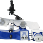
Need A Wafer Cutting Review?
If you already know the wafer material, diameter, thickness, and surface target, send the spec packet to DONGHE for a cutting-path review. Start with the silicon wafer cutting wire saw page for silicon lots, or move to the SiC and sapphire pages when the substrate is harder and more brittle.