Get in touch with DONGHE Company
-
Phone: +86 181-1645-5490
-
Email: Sales18@DongheScience.com

Silicon Wafer Cutting: Complete Process Guide
The cutting of silicon wafers is an unavoidable operation in the manufacture of semiconductors, the basis of all the modern world devices that are no longer able to do without technology. This article provides a very comprehensive account of the silicon wafer cutting process, where precision, methods, and tools are the main features that allow to meet the high standards set by the industry. No matter if you are an engineer, a scientist, or just a curious person, the article will be very interesting to you because it will lead you through the details of the wafer slicing explaining the main techniques like wire sawing and laser cutting while also covering the difficulties such as reducing kerf loss and achieving perfect cuts.
Introduction to Silicon Wafer Cutting
The cutting of silicon wafers is the first step that takes place in semiconductor manufacturing and consists of drilling silicon ingots to produce very thin and equal wafers for further treatments. The main purpose of this whole process is to get the highest possible accuracy and the best surface quality at the same time, hence the kerf loss, which is the amount of waste produced, is minimized. The two techniques mainly used for wafer cutting are wire sawing that involves the use of a very tight wire with abrasive slurry and laser cutting, which focuses on laser beams for high accuracy. Both of these methods are very carefully supervised to ensure that the produced wafers would fully meet the strictest industry standards for thickness, flatness, and surface quality.
What is a Silicon Wafer?

Silicon wafers are one of the main components in the creation of semiconductors and microelectronic devices. They are essentially thin organized slices of silicon. The ultimate source of these wafers is the high-purity silicon, which is normally supplied in the form of cylindrical ingots that are mechanically cut into disks of uniform thickness by various methods such as wire sawing or laser cutting. The process of making silicon wafers involves several rounds of polishing in which the surface is made light and mirror-like. The polishing grade silicon is then checked and examined against the most demanding specifications in the industry for parameters like thickness, flatness, and defect density, ensuring that they will perform the best in electronics as components.
Silicon wafers serve as the foundation for the microelectronics that are assembled on them through the processes of doping, etching, and deposition. The most frequently used diameters of silicon wafers range from 25 mm to 300 mm, with the size being application-dependent and the larger ones being suitable for chip mass production. The requirement for silicon wafers in various applications such as processors, memory chips, solar cells, and sensors, indicates the significant role they play in the growth of current technology.
Importance of Wafer Dicing in Semiconductor Manufacturing
Wafer dicing is the crucial process of the semiconductor manufacturing line by which silicon wafers are sliced into single dies or chips, which in turn are used in electronic devices, with very precise cuts. The function of this process is to eliminate the dies that, for example, are too thick, rough, or simply not accurate enough which affects the reliability and performance of the final product. The advanced dicing methods such as laser cutting and stealth cutting are increasingly replacing the traditional mechanical sawing method due to their capability of eliminating not only kerf loss and micro-crack formation but also of preserving the delicate wafer structures.
Industry Trends
The current trends in the semiconductor industry indicate that the introduction of the new dicing processes is mainly a result of the necessity to unlock the mentioned areas of miniaturization, increased die density, and advanced packaging methods like system-in-package (SiP) and wafer-level packaging (WLP) embracing. In addition, the precision and the dicing process’s efficiency still play a vital role in the same high-quality output being guaranteed, due to the fact that semiconductor devices are gradually being deployed in more and more applications that require high-performance and high-reliability, such as 5G infrastructure, automotive electronics, and IoT devices.
Overview of the Cutting Process
Semiconductor manufacturing cutting, especially wafer dicing, has undergone great changes and developed new capabilities to satisfy the demands of modern applications. The whole thing is done by accurately cracking the semiconductor wafers to get the individual dies, which presupposes that certain cutting techniques combining mechanical, laser, or plasma, will be employed depending on the composition of the material and the set specifications. The most recent developments have concentrated on coupling laser dicing to achieve higher precision and cleaner cuts, especially for fragile materials like silicon carbide (SiC). This is very important for the high-reliability areas like automotive and 5G technologies where even tiny defects can cause the whole device to fail.
Types of Silicon Wafers
Silicon wafers can be categorized very generally depending on their crystalline structure and doping type as follows:
1. Monocrystalline Wafers
These wafers are made of a single piece of silicon crystal with high uniformity and efficiency. They are mainly used in such areas as semiconductor devices and good solar cells where performance is of utmost importance.
2. Polycrystalline Wafers
These are made of many small silicon crystals and are much cheaper to make than monocrystalline wafers. However, they do not have as high a performance as their more expensive counterpart. Their main application is in the production of solar panels where cost is an important factor.
3. Undoped (Intrinsic) Wafers
Wafers consisting of pure silicon, with no foreign materials added on purpose, are the most expensive ones. The main application of such wafers is research and very small specialized applications.
4. Doped (Extrinsic) Wafers
Such silicon wafers are made of conducting materials (either p-type or n-type) that result from the introduction of certain impurities, for example, boron and phosphorus, respectively. These wafers play a vital role in the production of semiconductors and electronic components.
The selection of each wafer type is based on the specific requirements of the application, and a careful balancing of cost, performance, and material properties has to be done.
Monocrystalline Silicon vs. Polycrystalline Silicon
Monocrystalline silicon ensures greater efficiency and a homogeneous structure but polycrystalline silicon enables lower production costs and simpler manufacturing with the drawback of a little bit of performance loss.
Characteristics of a Si Wafer

Silicon wafers have some specific features that are strictly related to their application in the semiconductor and photovoltaic industries, hence, they are also referred to as the thin slices of silicon crystals that are inevitably linked with microelectronics. The key properties include the following:
- •
Crystalline Structure – Wafer forms the majorly single crystal or multi-crystal structures. The single crystal wafers offer the best electrical characteristics because of the uniformity of the lattice structure while the multi-crystal ones are cheaper and can meet the moderate demand of the low-power applications. - •
Electrical Conductivity – By the introduction of doping elements like phosphorus or boron the silicon wafers gain, the electrical conductivity according to the semiconductor type, which is the basic requirement for p-type or n-type semiconductors. - •
Thermal Stability – Silicon is one of the elements that have a very high melting point and excellent thermal conductivity, hence it can be trusted in very high-temperature conditions. - •
Optical Properties – For solar cells, silicon is the semiconductor material to get because of its very efficient light absorption quality, particularly in the case of single crystal ones, which is why they are offered with very high conversion efficiency. - •
Surface Polish and Thickness – The wafer surface is polished to a nanometer scale precision to minimize the defects and irregularities. The thickness is tailored to the application, usually between 150 µm and 300 µm. - •
Durability and Lifespan – Wafers, particularly the single crystal ones, are marked with long working lives due to their being structurally stable and at the same time resistant to degradation.
The mix of these characteristics is the key factor that makes silicon wafers essential in areas such as computing, renewable energy, and telecommunications; thus, they continue to be the material backbone of technology in the modern world.
Applications of Silicon Wafers
Silicon wafers are incredibly important to different sectors because of their amazing properties and perfect engineering. Here are the five primary applications of silicon wafers and a detailed description of how they are used:
1. The Semiconductor Industry
Silicon wafers are the foundation of integrated circuits (ICs), which are the hearts of all electronic devices. These wafers are the basis for the creation of transistors, diodes, and microchips used in computers, smartphones, and other consumer electronics. For example, current logic chips in CPUs and GPUs rely on features that are created in nanoscale on silicon wafers to function at high performance and also be energy-efficient.
2. Photovoltaic Cells
The non-silicon renewable energy sector is heavily dependent on silicon wafers for the production of photovoltaic (PV) cells. These cells convert sunlight into electric power and are made from monocrystalline silicon, which is yielding their outstanding efficiency. The everlasting increase in the use of silicon panels within the solar power market is being more and more reported night and day, with silicon-based panels claiming over 95% of the market share globally as they are chosen for their reliability and affordability.
3. MEMS Devices (Micro-Electro-Mechanical Systems)
Silicon wafers are the substrates for MEMS devices that make various devices like accelerometers, pressure sensors, and gyroscopes. These devices are all over the place; they are used in automotive, aerospace, and medical industries for example—airbag sensors and smartphone motion sensors are made on silicon wafers.
4. Telecommunications
Silicon wafers are vital for producing RF (radio frequency) components and photonic devices that are used in telecommunications. They enable technologies such as the 5G network, fiber optic systems, and satellite communication, which demand the highest data transmission speed and reliability.
5. LED Technology
With the advent of eco-friendly lights, silicon wafers have become a key player in LED manufacturing. The use of silicon wafers as substrates for the GaN (gallium nitride) layers contributes to LED manufacturing cost-cutting and at the same time supplying thermal stability and performance.
These applications highlight the versatility and indispensability of silicon wafers in multiple domains, which makes them basic material for the technological development of our time.
Wafer Dicing Techniques
Wafer dicing is a process that involves the cutting of semiconductor wafers into single dies or chips with great precision and also efficiency. The cutting techniques which are the most widely used are as follows:
Blade Dicing
This process uses a diamond-tipped saw blade to make a cut through the wafer. It is a very effective method for conventional wafers and gives very good cuts in terms of accuracy, albeit it might cause the material to suffer from physical stress or micro-cracks.
Laser Dicing
In laser dicing, highly focused laser beams are used to vaporize the wafer along predetermined lines. This method has the advantage of being non-contact, which ultimately results in less material destruction and thus is applicable to thinner or more fragile wafers.
The selection of both methods is influenced by wafer material, thickness, and desired accuracy among other factors.
Overview of Dicing Technology
The semiconductor industry has always been a leader in the innovation scene and so dicing technologies have changed only to be able to provide the highest levels of accuracy, speed, and at the same time produce minimal waste. Present-day studies and recent results indicate that hybrid dicing has become the first choice in the industry where mechanical sawing is used along with laser dicing in order to attain great efficiency. This solution gives producers the possibility to capitalize on the advantages of both—the dependability of the mechanical sawing and the non-destructive characteristic of the laser dicing for fragile materials such as ultra-thin wafers.
Moreover, the newest industry trends are pointing out the need for dicing systems that are capable of being flexible and are powered by AI monitoring and real-time adjustments. The aforementioned features play a significant role in the precision by self-regulating to the variations in wafer properties or environmental factors, hence the quality of the production batches is kept. This is extremely crucial in the manufacturing of cutting-edge microelectronics such as MEMS and 3D ICs, where even the tiniest imperfections might lead to the devices being non-functional.
Therefore, the modern dicing technology, mixing old skills and new inventions, still plays a great role and becomes the master of semiconductor devices production with marvelous performance.
Detailed Dicing Methods
Blade Dicing
Blade dicing is a highly precise process to divide semiconductor wafers into die or chip forms. A diamond, for example, is one of the materials used to make the high-speed rotatingblade, and the slicing actions through the wafer are executed in an absolutely accurate and steady manner. Blade dicing is known for its ability to make clean and straight cuts; this is why it is selected in the applications that require very high precision. Additionally, the modern controls in the blade dicing machinery make it possible to customize the cutting parameters according to the wafer’s material composition and thickness, thus ensuring that the best quality is achieved. It has nevertheless remained one of the most reliable methods of cutting in semiconductor manufacturing.
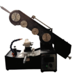
Wire Saw Dicing
Wire saw dicing is an extremely accurate cutting practice primarily used for the separation of semiconductor wafers and other fragile items. It makes use of a thin wire, normally laden with abrasive materials, to create a non-stop cut in the substance. Among the numerous advantages of wire saw dicing, one of the most significant is the ability to work with large, delicate wafers that experience minimal material loss and have very little risk of damage. The process is particularly suitable for applications that require very high accuracy and where it is very critical to maintain the surface quality, like in the production of advanced electronic components.
Laser Dicing
Laser dicing is a very accurate method that cuts semiconductor wafers and other materials by directing a laser beam to a specific cutting path. This process utilizes the laser’s capacity to provide high energy to very precisely separate the material with the least possible kerf width and heat-affected zone. It is particularly suitable for materials that have complex shapes or that need very thin cuts, thus it is the best choice for microelectronics and device manufacturing. On top of that, laser dicing reduces the risk of contamination because it is a non-contact method, thus guaranteeing high-quality outcomes and higher yield rates.
Plasma Dicing
Plasma dicing is a cutting-edge, non-destructive separation technique for semiconductor wafers that yields a great number of chips. It makes use of a process called reactive ion etching (RIE) to remove the material along the scribe lines that have been predetermined. This method removes the drawbacks of conventional dicing methods, namely, mechanical stress and generation of particles, thus providing the die with better quality and reliability. Plasma dicing is a preferred method for very thin wafers and narrow streets because it permits the maximum number of good dies per wafer while supporting their physical integrity.
Stealth Dicing
The stealth dicing method eliminates the use of a laser for cutting silicon wafers and other materials. However, lasers are still applied to make subsurface alterations along the predefined scribe lines, but they do not reach the top layer of the wafer. This gentle treatment brings about hardly any surface chipping or cracking and thus the quality of the dies is improved. The process is particularly suited for fragile materials and very thin wafers as it provides higher accuracy and at the same time the wafer is intact, which is a big advantage. Moreover, stealth dicing has a positive effect on the environment as well, for it almost completely eliminates the production of debris and doesn’t require water or abrasives, thereby reducing the risk of contamination.
The Wafer Dicing Process

Wafer dicing refers to the splitting of semiconductor wafers into separate chips or dies. The operation involves making exact cuts along the lines that identify each die. The three main methods of dicing are mechanical sawing, laser cutting, and stealth dicing, with the material’s properties and the application’s requirements determining the method to be used. The procedure is characterized by the need for utmost precision which is not only a prerequisite for the dies to remain whole but also for them to perform efficiently in the next electronic applications. Moreover, the cutting-edge techniques are meant to reduce the damage, waste, and material loss to such an extent that the final product is of high quality.
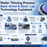
Preparation of the Silicon Wafer
Certain significant activities make up the entire process of silicon wafer production, thus yielding the requested immaculate quality for the semiconductor industry. The first step, either Czochralski or float-zone technique purifies raw silicon which results in extremely pure monocrystalline silicone. Diamond-coated wire saws are used to cut the silicon ingot into very thin wafers taking into account the kerf loss and surface irregularities as part of the thickness accuracy. The wafers are then subjected to Chemical Mechanical Polishing (CMP) which involves both chemical and mechanical polishing to the extent of over ten times smoother than the surface of glass.
During the whole process, modern etching as well as the cleaning methods have been applied to ensure the removal of both large and very small latent particles. Hydrofluoric acid solutions are the standard ones used to remove the natural oxide layers from the wafer while protecting the silicon substrate. In addition, edge treatment may be performed to prevent defects and breakage during subsequent handling. The wafer preparation stages are monitored very closely to different surface roughness, wafer thickness and flatness parameters that can meet the extreme standards set for semiconductor devices. This, in turn, guarantees their reliability and efficiency in such areas of application as consumer electronics, advanced artificial intelligence and more.
Optimal Cutting Parameters
Optimal cutting parameters are major factors that directly determine the quality, accuracy, and productivity of wafer dicing processes in semiconductor manufacturing. The defining factors usually comprise spindle speed, feed rate, blade thickness, and coolant flow rate, each of them need to be calibrated very precisely according to the wafer’s material properties and the final device’s requirements. For example, higher spindle speeds may give the advantage of better cut quality but their effect on heat generation results in thermal damage preventing the required optimized coolant flow. In the same manner, cutting with slower feed rates results in less chipping and micro-cracks, however, it tends to limit throughput and the scalability of the process.
AI-Powered Optimization
As per the most recent data and studies, adoption of state-of-the-art AI-powered tools for continuous cutting parameters’ monitoring and adjustment has been associated with huge process gains. Such systems process sensor signals to keep the best possible conditions, thereby facilitating the achievement of little material wastage and excellent edge quality. The extent of this optimization is paramount in satisfying the needs of the new-generation technologies like 5G, autonomous cars, and AI hardware, where even a slight variation in wafer quality could lessen the performance of the device.
Cleansing and Handling After Dicing
The wafer that has been sliced up into pieces must be cleaned completely after that operation in order to keep its quality and to prevent the contamination that might alter the following production process. The dicing process leads to the generation of silicon dust, waste, and possibly cutting oil residues as its by-products. Wafer cleaning procedures that incorporate megasonic or ultrasonic cleaning are among the most sophisticated and economical methods available. They consist of using sound waves with extremely high frequencies to effectively break the bonds between the dirt particles and the surface of the wafer, but at the same time they do not apply any harmful stresses to the wafer.
For the safe handling of the wafer, more and more of the automated systems with no-contact handling features are getting adopted in the precision areas. Such systems do limit very much the likelihood of both the mechanical stress that would be imposed and the contamination that would come about through the operator. Moreover, the very strict cleanroom conditions in the area of post-dicing are regulating the inflow of airborne particles. The trends in searches and the insights into the industry show that keeping the cleanliness level ideal and proper wafer handling are turning into highly crucial aspects as the size of the devices continually goes down, where even minute contaminants at the nanoscale may cause dysfunction.
Challenges in Wafer Cutting

Wafer cutting entails a number of significant difficulties that to be taken care of in order to keep the accuracy and the number of defects to a minimum. Among the major concerns are the slicing going on with the material whereby micro-cracks or notches might be formed that would render the wafers not structurally reliable. Holding the aforementioned tolerances to very small limits and surface finishes that are very smooth is another difficulty, especially with the continuing reduction in device sizes. Moreover, keeping contamination from debris at a minimum and maintaining tool wear at a consistent level are very important in order to prevent defects from being introduced that could impair the performance of the devices in their advanced applications. To beat these barriers, there is a need for the effective monitoring, precise calibration of the equipment, and utilization of the advanced cutting technology.
Common Issues in the Cutting Process
- ▪
Tool Wear and Degradation – Continuous cutting tool wear results in a decrease of precision and quality of the surface thus demanding frequent replacement or maintenance for the tools to keep delivering good performance. - ▪
Material Deformation – Softer materials during cutting operation may get deformed instead of being cut-off cleanly, leading to wrong dimensions or lower quality. - ▪
Heat Generation – The excessive heat resulting from friction during cutting can change the characteristics of the material, causing thermal damage or distortion. - ▪
Burr Formation – The occurrence of rough edges or burrs on the workpiece can take place, which will require additional finishing steps to comply with the quality standards. - ▪
Contamination and Defects – The accumulation of garbage or improper cleaning during cutting can create defects that will negatively impact the overall reliability of the finished product. - ▪
Machine Calibration Issues – Out of alignment or incorrectly calibrated machinery will cause dimensional mistakes and need realignment to recover cutting precision.
Impact of Material Properties on Dicing
The dicing process in terms of both efficiency and precision is significantly influenced by the material properties. The operation can be greatly impacted by the different characteristics of the material that is being diced. The following five properties of the materials and dicing impact are discussed:
1. Hardness
Among the hardest materials are sapphire or silicon carbide, which need durable cutting tools and finally increase wear of the tool. To successfully cut these materials, diamond-coated blades or lasers are commonly used. The hardness also correlates to the speed of cutting and cooling requirements.
2. Brittleness
High brittleness materials, for example, certain ceramics or glass, are usually chipped and cracked during the dicing process. This compels the cutting parameters to be optimized, lower feed rates to be practiced, and special blade designs to be employed so as to minimize damage and ensure precision.
3. Thermal Conductivity
Low thermal conductivity materials, for instance, some polymers and silicon, are capable of retaining heat during the cutting process, thus delivering thermal stress and microcracking. To eliminate heat buildup, it is vital to provide adequate cooling that can be executed through either liquid or air systems.
4. Grain Structure
Polycrystalline materials with random grain distributions, like metals or composite materials, will sometimes become the reason for fluctuating cutting performance. A suitable blade must be selected that can cope with varying density, and employing vibration dampening might be necessary.
5. Thickness Variability
Dicing faces blade instability and depth control caused by an uneven distribution of thickness across the material. Such variability can result in either incomplete cuts or inaccurate cuts, which, in turn, requires the machine to be extremely precise in calibration, and height sensors that can dynamically adjust in real time.
Knowing the material properties and being capable of handling them in the dicing process result in higher product quality, fewer defects, and longer tool life.
Solutions to Dicing Problems
By applying machine settings optimization and the use of high-end tools, I can deal with dicing problems properly. I use blades with the right bond composition for material hardness which is observed constantly for not to getting excessive wear. I am changing feed rate and cutting speed in dealing with brittleness while still using coolant to reduce thermal stress. For abrasive materials, I am using diamond blades of a higher grade and am doing regular maintenance to prolong the tool life. For dealing with impurities, I am using precise filtration systems to keep the cutting fluids clean and thus reduce the risk of contamination. Finally, I can dynamically calibrate the machine through thickness variability management using real-time sensors to produce cuts that are consistent as well as accurate. All these actions together result in getting high precision, fewer defects, and more operational efficiency.
Future Trends in Silicon Wafer Cutting

Emerging trends in silicon wafer cutting are mainly about precision, efficiency, and sustainability. USB-based cutting technology is a new feature in this context that is very effective in material-saving, and it can also produce ultra-thin wafers with the highest precision. Besides this, AI-enabled machines in cutting processes perform defect detection and optimization on-the-fly, thus resulting in less downtime and better yield rates. Exploration of new abrasive materials and technologies is ongoing in the industry to not only improve edge quality but also to lower overall costs at the same time. Automation innovations and installation of smart manufacturing systems are further causing the workflows to be more efficient, the production cycles to be faster, and the energy consumption to be lower. In sum, these changes are a step ahead the ongoing evolution to get very efficient and thus sustainable wafer cutting solutions.
Advancements in Dicing Technology
The latest developments in the field of dicing technology have mainly focused on increasing precision, efficiency, and material integrity. The use of laser dicing has been a major factor in speeding up the processing while at the same time minimizing damage in fragile wafers by the formation of microcracks. Moreover, plasma dicing has been welcomed for its capability to yield higher quantities and to leave edges that are cleaner than in the case of using other methods, which is particularly important in the case of very densely packed semiconductor designs. Newer and better blade materials and coatings have also contributed to the resistance of wear and the accuracy of cutting being improved and so the lifetimes of the tools being lengthened and the costs of operation being cut. All these advancements together break down the barriers in the manufacturing of semiconductors of the highest quality with the most productivity possible.
Impact of Industry 4.0 on Semiconductor Manufacturing
Industry 4.0 has redefined semiconductor manufacturing through the integration of such paradigms as automation, data analytics, and machine learning. The application of these technologies has resulted in the substantial improvement of the processes involved in semiconductor manufacturing, which have become more efficient, accurate, and scalable. The following list gives an overview of the main five impacts of Industry 4.0 on semiconductor manufacturing:
- Real-time Data Analytics: Advanced data analytics systems enable manufacturers to analyze performance metrics in real time. This capability allows for the rapid identification of defects, bottlenecks, or deviations from expected performance parameters, thereby reducing wastage and increasing yield.
- Predictive Maintenance: The combination of artificial intelligence (AI) and IoT-enabled sensors has made it possible for predictive maintenance systems to foresee equipment failure and thus take action before it happens. Consequently, there is a significant reduction in downtime, and the life of costly, complex machinery is prolonged.
- Process Automation and Robotics: Automation technologies and robotics have been employed to take over the consistent and high-quality production of semiconductor components by reducing the time taken for wafer handling and lithography. Furthermore, the use of robotic systems in the ultra-clean environments helps in reducing the risk of contamination.
- Smart Supply Chain Management: Industry 4.0 applies digital twins and IoT to supervise and fine-tune the activities of the supply chain. The result is less inventory, shorter lead times, and enhanced operational efficiency, overall.
- Machine Learning for Process Optimization: Machine learning techniques are used to analyze the enormous amounts of data produced during the manufacturing process in order to detect ongoing patterns and thus suggest improvements. This results in tighter process control, shorter cycle times, and better resource utilization.
The positive aspects of these advancements combined together, demonstrate that semiconductors manufacturing has greatly benefited from Industry 4.0, as the latter has provided a fount of innovations, increased the volume of production and at the same time allowed the maintenance of the top quality standards in the rapidly changing field.
Emerging Technologies in Wafer Cutting
Precision, efficiency and yield are the main principles directing the development of new technologies in wafer slicing. One of the main trends in this field is the use of laser cutting, which causes no mechanical stress on the wafers at all, and we can add to that plasma cutting, which provides perfect edge quality and stronger dies. Moreover, these materials processing technologies along with sophisticated metrology and automation have made it possible to have minimum material losses and at the same time cope with the demands of the increasingly complex smallest and most advanced semiconductor designs.
Frequently Asked Questions
What is the major reason behind slicing silicon wafers?
The major reason for wafer slicing is to change the form of a big cylindrical silicon ingot to thin uniform discs called wafers. This procedure is a vital part of semiconductor manufacturing. Wafers are mainly used as substrates for integrated circuits and solar cells, so it is crucial to get the thickness accurately, and the surface quality very high, while keeping the material’s crystallographic integrity.
What cutting techniques are applied the most for silicon wafers?
The multi-wire sawing (MWS) method is mainly adopted by the industry. This method employs a thin wire web that is moving at high speeds for cutting the ingot. The main variations that exist within this category are:
- Loose Abrasive Sawing (Slurry): Employs a plain wire that carries a slurry mixture of oil and abrasive particles (like silicon carbide).
- Fixed Abrasive Sawing (Diamond Wire): This method uses a wire that is embedded with diamond particles. Because of its quicker and more effective cutting performance, this method has largely taken the place of slurry sawing.
What makes diamond wire sawing a more popular choice to traditional slurry processes?
Diamond wire sawing presents a number of considerable benefits in manufacturing settings. The cutting mechanism of the fixed abrasive diamonds is more forceful and rapid than the rolling action of loose slurry. This leads to incremented throughput and productivity. Furthermore, diamond wire sawing creates less waste and does not require disposal of hazardous oil-based slurry mixtures which are characteristic of older methods.
What is the term “kerf loss,” and why is it essential to limit it?
Kerf loss is the term used to describe the quantity of high-purity silicon that is turned to dust and lost during the cutting process. Since manufacturers consider kerf loss a major factor when determining their silicon inventory and costs, there is always a strong drive to minimize it. The use of smaller diameter diamond wires is one of the ways through which manufacturers are able to create narrower cuts and in turn preserve more silicon for the actual wafers.
How are wafer slicing and wafer dicing different from one another?
Even though both techniques involve cutting, they are performed at different points in the production cycle:
- Wafer Slicing: The process takes place at the beginning of semiconductor manufacturing, which is the cutting of the raw silicon ingot into discs (wafers) of blanks.
- Wafer Dicing: The process is done at the end of the production cycle. After the wafer fabrication and the circuits’ printing on it, dicing separates the wafer into individual chips or dies for further packaging.
What distinguishes laser dicing from mechanical blade dicing?
On the one hand, the laser dicing (also referred to as stealth dicing) is a non-contact method in which a focused beam is used to create a modified layer within the silicon without affecting the surface. The wafer is subsequently stretched to isolate the chips. The reduced width of cutting lanes (streets) and thus lesser chances of damaging sensitive circuitry are the benefits of this method.
On the other hand, the mechanical dicing involves a fast-spinning diamond blade that cuts the wafer physically. Though it was effective, it did lead to some mechanical stress and surface chipping.
What advantage does the coolant have during the wafer-cutting process?
The coolant is important to the cutting operation as it is helpful in keeping both the cutting tool and the silicon material in good health structure-wise. During the cutting process which generates a lot of heat, the friction caused during cutting is the main reason why the heat is too much. In order to cool the silicon and prevent it from warping or cracking, a continuous flow of coolant is needed. Additionally, the cooling water carries away the silicon particles and waste that are left after cutting making sure that the cut is clean and there is no jamming of the cutting tool.
Reference Sources
- How are Silicon Wafers Cut?
In this article, the main slicing methods, which include wire sawing, ID sawing, and multi-wire sawing, are described - The Ultimate Guide to Wafer Dicing
It is a complete guide to wafer dicing that covers all aspects of the process, such as techniques, challenges, and innovations in the separating of individual integrated circuits (ICs). - The Complete Guide to Monocrystalline Silicon Wafer Cutting
The guide is dedicated to the monocrystalline silicon cutting method, primarily diamond wire saw cutting machines. - The Future of Semiconductor Manufacturing
Modern wafer dicing techniques are highlighted, including Water Jet Guided Laser Dicing, a high-precision method that fuses laser cutting with water jet cooling. - Recommend reading: Hard and Brittle Material Cutting Wire Saw | Precision Diamond Wire Saw Machine
The references mentioned above give a detailed overview of the silicon wafers cutting related processes and the technological advancement.