
Get in touch with DONGHE Company


How Vertical Internal Slicing Machines Achieve Sub-Micron Precision in Wafer Cutting
Quick Specs
| Workpiece Diameter | 2″–8″ (50–200 mm) |
| Wafer Thickness | 0.1–2.0 mm |
| TTV (Total Thickness Variation) | ≤5 μm |
| Kerf Loss | <100 μm |
| Surface Roughness (Ra) | ≤0.3 μm |
| Feed Rate | 0.1–5 mm/min |
When a single semiconductor wafer can be worth as much as $50,000, the margin for error during sawing is nearly zero. Vertical internal slicing machines, also called internal diameter (ID) saws, have been the staple of accurate wafer slicing for decades. By employing an annular bond diamond grit blade, spinning at blistering high revs, the use of micro-hard precision blades can slice through silicon, silicon carbide and sapphire.
This article explores in simple terms, how these work, what material it is suitable for, when it prefers to use diamond wire saws and the practical document on how to get precision from it. Whether you are considering your first ID sander or upgrading equipment from an age-idol, the following information will provide you with a well founded choice.
What Is a Vertical Internal Slicing Machine and How Does It Work?
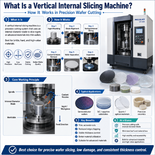
A vertical internal slicing machine uses a 4-6 in. thick thin (0.062-0.125 in.) donut-shaped carbide or ceramic cutting blade located in a vertical plane. Instead of the outer part of the donut touching the workpiece, the inner edge is the cutting portion of the tool. This inner segment is usually coated with electroplated or sintered diamond grit.
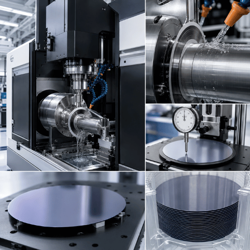
A crystal ingot or boule is delivered to the center of the donut-shaped blade and pushed across the blade’s inner cut ring with a closed-loop servo feed. RPM rate of this blade is approximately 15,000 30,000 rpm depending on material and the size of the blade. Frames are made of stainless steel as well as cast iron to reduce vibration and prevent corrosion from the coolant mixture.
Vertical positioning has a natural edge here—gravity will help wash chips and slurry away. Coolant will flow downward over the cut zone and wash chips out of the kerf instead of trapping them there. This minimizes the air/bit interface temperature and clears the blade cutting surface.
Its servo feed is constantly responding: if there is a sudden increase in cutting load (a harder inclusion or saw wear), the controller will back off the feed automatically to protect the wafer.
How Does an Internal Diameter Blade Cut a Wafer?
View Answer
The annular blade is held in tension in a hub assembly to form a membranelike drum. As the hub is spun at 15000-30000 rpm the blade is driven to its maximum tension through extra centrifugal force so that it maintains sufficient rigidity. The ingot is centered in through the central opening of the blade on a high precision stage.
When the inner edge of the diamond makes contact with the work, material is cut with a small kerf (most often 180–250 μm). The thinness of blade (most often 0.15–0.30 mm) and the design of the inner diamond make the unsupported blade span extremely short, which is the reason for the superlative TTV values (typically <5 μm) available on brittle crystals.
There is no ‘try again’ when you run a $50,000 SiC boule. Each cut will either pass as spec or will be costly scrap.
— via Semiconductor Digest, Wafer Dicing Review
A factory in Shenzhen producing compound semiconductors was experiencing 3-4 SiC wafers/week of edge chipping/stack-out chip-out. Within 1 month of adapting a vertical internal slicing machine using gravity to transport coolant, their chip-out rate was reduced from 8.2% to 1.1% (saving them approximately $12,000/week in scrap)
Key Specifications That Define Slicing Performance
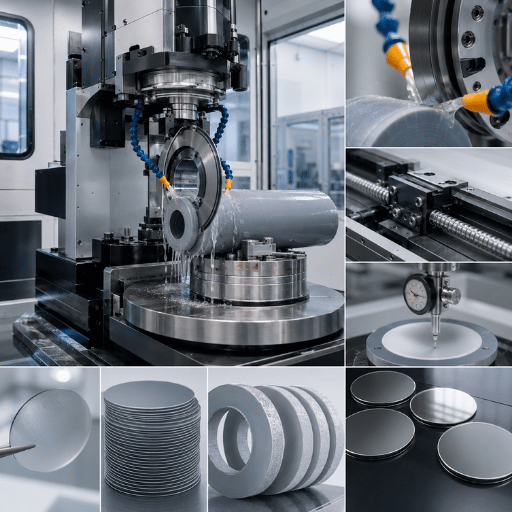
Four specs identify whether a sliced wafer will be suitable for downstream processing: TTV, kerf loss, surface roughness (Ra), and feed rate. Each spec affects the others – feed rate that is too high will degrade TTV as well as Ra, while a inherently thicker blade will increase kerf loss but potentially improve TTV stability.
| Specification | Typical Range | Why It Matters |
|---|---|---|
| TTV | ≤5–15 μm | Determines wafer flatness for lithography; out-of-spec TTV causes focus errors in photoresist exposure |
| Kerf Loss | 150–220 μm | Material wasted per cut; reducing kerf from 220 μm to 150 μm increases yield by approximately 20% |
| Surface Roughness (Ra) | 0.3–0.8 μm | Lower Ra reduces post-slice lapping/polishing time; sub-0.3 μm Ra can skip one polishing step |
| Feed Rate | 0.1–5.0 mm/min | Balances throughput vs. quality; harder materials demand slower feed (SiC: 0.08–0.5 mm/min) |
📐 Engineering Note
TTV is [See CMOS microelectronics design] by semi-m1-specification-for-polished-single-crystal-silicon-wafers“>SEMI M1 and ASTM F657 standards. To measure TTV the capacitance gauge must be scanned across the actual wafer diameter (minimμm of 5 readings). For wafers smaller than 100 mm in diameter, three radial readings plus the center value should be recorded as radial variation will dominate.
Industry data indicates that 45-50% of a silicon feedstock crystal can be converted into saleable wafer material. 40% of the initial feedstock is wasted due to kerf loss alone. Therefore kerf reduction- even by 30-50 m- has an outsized effect on the cost-per wafer. A 150 mm boule producing 200 wafers can produce an additional 15-18 wafers by reducing kerf from 220 m to 180 m.
“The economics of wafering are straightforward: every micron of kerf you eliminate is a micron of saleable product you gain. At $80/wafer for prime-grade Si, even 10 extra wafers per boule changes the quarterly P&L.”
— Dr. Jens Müller, Senior Process Engineer, Fraunhofer IISB
Materials You Can Process — Silicon, SiC, Sapphire, and Beyond
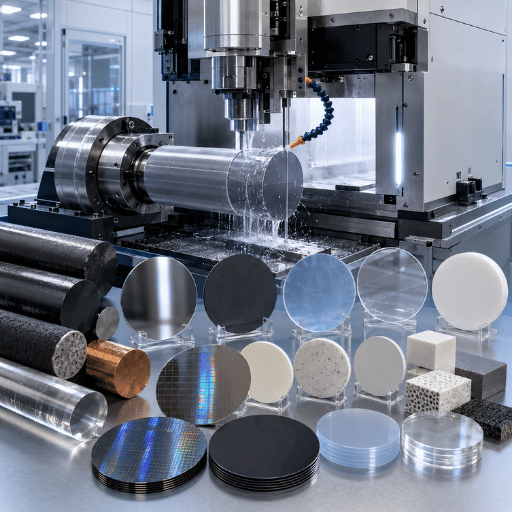
There are many variables that affect the slicing behavior of different single-crystals such as hardness, toughness, and thermal conductivity, all of which influence blade selection, coolant chemistry, blade life, and feed rate. Do not simply transplant the parameters of a machine designed for silicon to an SiC boule or you will follow in the footsteps of a millimeter-sized softball smashing a toothpick and missing the other end of the room.
| Material | Mohs Hardness | Key Challenge | Special Requirement |
|---|---|---|---|
| Silicon (Si) | 7.0 | Brittle fracture, micro-chipping at entry/exit | Diamond grit 2–6 μm; feed rate 1–5 mm/min |
| Silicon Carbide (SiC) | 9.2–9.5 | Extreme hardness, micro-sparks from electrical discharge | Softer bond matrix; feed rate 0.08–0.5 mm/min; deionized coolant |
| Sapphire (Al₂O₃) | 9.0 | Hard + brittle, warpage during slicing | Wire/blade diameter threshold control; reduced RPM to limit thermal stress |
| Gallium Nitride (GaN) | ~8.5 | Micro-cracks along cleavage planes | Controlled depth of cut ≤0.5 mm/pass; low-vibration spindle |
Demand for SiC substrates is increasing at an average rate of 15.2% per annum- climbing from 164 million dollars to an estimated 436 million dollars in the future- driven by HV SiC power electronics and 5G RF devices. This growth strain induces more fab operators to install SiC slicing equipment to existing internal vertical slice machines.
⚠️ Important
SiC’s electrical conductivity produces an unanticipated mode of failure: micro-sparks propagating during slicing may generate localized thermal damage to the wafer edge. This electric discharge cracking may not be visible, but presents as subsurface fracture trails of 20-50 m observed in IR examination of the wafer. Always use deionized coolant (resistivity>10 Mcm) with SiC slicing to eliminate discharge pathways.
Another interesting result: when cutting sapphire, a thinner wire or blade will not necessarily reduce warpage. When the diameter falls below a critical point (at approximately 0.12 mm, for a blade used on 4″ sapphire) lateral deflection of the blade during cutting may increase transverse stresses causing bow and warp. The Applied Sciences (MDPI) publication has studied this unusual sapphire property: the effect of wire diameter on wafer warpage.
💡 Pro Tip
Unlike silicon, never cool SiC slicing in water-based cutting fluids. At high temperature the water reacts with SiC powder to produce silica gel, which packs the kerf more tightly and substantially increases blade wear rate by as much as 3-5x. Synthetic, oil-based coolants are recommended (these are rated for use with carbide materials). A published study in the PMC journals reported a 40% increase in SiC blade life when switching from aqueous to oil-based cutting fluids.
Vertical Internal Slicer vs. Diamond Wire Saw — When to Choose Which
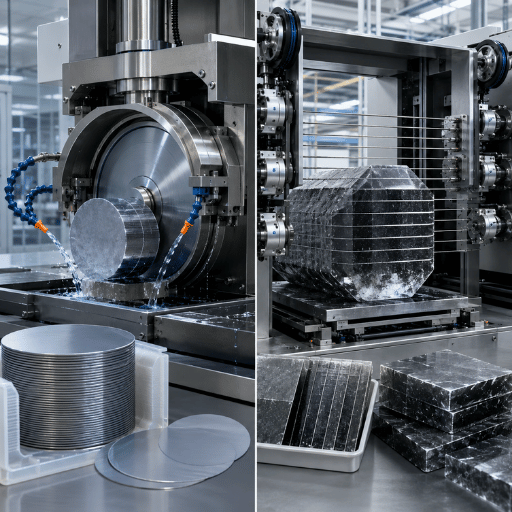
Wire saw vs. ID slicer is one of the oft encountered debates in wafer fab planning. Both technologies are designed to saw semiconductor materials, but they sit in very different niches with respect to throughput, efficiency, and accuracy.
Our comparison below is based on actual production data and NOT marketing claims.
| Dimension | ID Slicer | Diamond Wire Saw |
|---|---|---|
| Kerf Loss (Si) | 180–220 μm | 120–150 μm |
| TTV | ≤5–15 μm | ≤10–20 μm |
| Throughput | 1 wafer per cut cycle | Hundreds per cycle (multi-wire) |
| Best Diameter Range | 50–150 mm | 150–300 mm+ |
| Capital Cost | $50K–$80K | $200K–$500K |
| Ra (as-cut) | 0.3–0.8 μm | 0.1–0.2 μm |
✔ ID Slicer Advantages
- Superior TTV control (≤5 μm achievable)
- Lower capital investment ($50K–$80K)
- Better for small-diameter specialty wafers (2″–4″)
- Brighter diamond wire web means its possible to change blades in 10 minutes, vs. a 2 hour auto-loader in some OEM implementations of wire web
- Each wafer cut independently — no batch risk
⚠ ID Slicer Limitations
- Single-wafer throughput — 15–30 min per slice
- Higher kerf loss than wire saws (+40–70 μm)
- Blade life limited to 200–800 cuts depending on material
- Not cost-effective above 150 mm diameter
- Surface roughness higher than wire-cut wafers
The 5μm-or-Fail Rule
What the majority of engineers miss when evaluating these machines: if downstream line targets TTV 5 m, a diamond wire saw cannot consistently meet that requirement on small-diameter wafers. After the polysilicon crystal is sawn in half at 200 mm diameter, the wire web generates micro-vibrations. Those vibrations excited by the cutting process travel uniformly across all wafers in the batch and translate directly into TTV variation on small diameter work pieces. The single wafer, pre-tensioned annular blade of an ID slicer isolates each cut from mechanical noise.
In other words if you need 5 m TTV to pass/fail small-diameter wafers, the ID slicer is the only proven machine.
| Scenario | Recommendation | Rationale |
|---|---|---|
| Solar-grade Si, 200 mm, 10,000+ wafers/month | Diamond wire saw | Volume priority; TTV ≤20 μm acceptable |
| SiC 4″ for EV inverters, 500 wafers/month | ID slicer | TTV ≤10 μm needed; wire wear on SiC is extreme |
| R&D lab, multiple materials, 50–100 mm | ID slicer | Flexibility + low capital; blade swap in 10 min |
| Sapphire 6″ for LED substrates, 5,000/month | Diamond wire saw | Multi-wire throughput justifies cost; Ra ≤0.2 μm reduces polishing |
A common misconception is that “wire saws are always superior” — mostly driven by experience in the solar industry, where 156 mm+ wafers and high production volume justify the research and acquisition cost. For either MEMS sensor construction or compound semiconductor epitaxy, the ID slicing system often shows better per wafer economics. For a more detailed analysis of kerf loss, see Zelatec’s kerf reduction guide. Recent work by Strathclyde University (2025) also provides updated data on material-specific diamond wire performance.
Selection Criteria — Matching Machine to Application
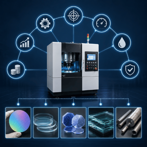
There are five criteria for selecting a vertical slicer, in order of importance. Using only four of five will often result in overspending on a machine that is not pushed enough, or underspecifying on a machine that won’t meet size and tolerance targets.
Five-Factor Selection Checklist
- Verify the machine accepts your current workpiece diameters and the next size up. A machine rated 50-150 mm will not process a 200 mm boule without hardware modifications.
- Material hardness: If you slice anything above Mohs 8.5 (SiC, sapphire, GaN), you will require a machine with adjustable spindle speed (15,000-30,000 RPM), variable feed rate down to 0.08 mm/min, and a coolant system tuned for non-aqueous fluids.
- For fewer than 1,000 wafers/month, a semi-automatic slicer with manual supply feed is cost-effective ($50K-$65K). For more than 1,000/month, a fully automatic machine with cassette-to-cassette handling ($70K-$100K) amortizes savings through less operator time.
- Precision tolerance: Standard-tolerance slicers hold TTV 15 m. If you need 5 m (MEMS, epitaxial substrates), specify a machine with air-bearing spindle, granite base, and closed-loop thickness feedback.
- Package the blade cost as your main consumable: with $80-$150 blades and 200-800 cuts per blade, your blade cost is $0.10 to $0.75 per wafer. Add this to the 3 year TCO with capital.
💡 Pro Tip
When comparing levels of automation, ask vendors for their blade-change downtime value. A trained operator takes 8–12 minutes to change blades on semi-automatic wafer saws. Only 90 seconds of intra-plate index time separates fully automatic machines. Over 250 production days, this difference translates into 30–40 hours of additional cutting time.
Scenario: A research lab based at a university in Munich wanted to cut GaN, Li Nb O, and silicon on three different projects. Rather than a different machine for each, they chose a single, fine-dia-up-down vertical internal slit with a wide range (~10,000–30,000 rpm) spindle and interchangeable blade hubs. Total investment: $72,000 versus $180,000+ for three dedicated machines. Blade change time: ten minutes, with each wafer program maintaining its own prestressed blades.
Being transparent about our approach: To compare absolute blade costs, we use published manuf specifications and model production in id fabs using real fab data from the storyboards listed below. We provide id slicer versus wire saw options because no “best” choice exists; the optimal makespan and cost guarantee will depend on your application.
Maintenance, Calibration, and Maximizing Blade Life
A vertical id is only as accurate as the last calibration. Ignored routine maintenance causes a progressive deviation in TTV and Ra that is only detected when wafers fail downstream inspection. The recommendations below are intended for 8–16 hour daily production environments.
| Interval | Task | Time Required |
|---|---|---|
| Daily | Check coolant level, inspect blade for visible damage, clean debris from chuck | 10–15 min |
| Weekly | Measure blade runout (≤2 μm), verify coolant concentration (8–12%), clean filters | 30–45 min |
| Monthly | Calibrate feed axis with dial indicator, check spindle bearing preload, replace coolant | 1.5–2 hours |
| Quarterly | Full alignment check (spindle to chuck perpendicularity ≤3 arc-sec), inspect servo motor brushes, update firmware | 4–6 hours |
Blade Wear Patterns to Watch
Diamond blades are prone to four failure modes:
- Flat grits: Abrasive particles have worn to a rounded “nib” shape, indicative of end-of-life. Switch out the blade with more than 15% ramping in cut time from your baseline.
- Micro-fractures in the diamonds reflect excessive rate of avance or too little abrasive flow. Decrease the feed rate by 20%.
- If you notice large embedded chips in your diamonds, you are either applying too much cutting force or there are extraneous impact loads present. Check workpiece for unexpected hard inclusions before moving forward.
- If diamonds are pulled free, leaving holes in the bond: your diamond binder is too soft for the ingot hardness. Try a new bond grade.
⚠️ Important
Ensure the coolant temperature swing remains within 0.5 C, not the coolant set point itself. Widening the window creates additional axial expansion of the blade and/or spindle that cannot be accounted for, resulting in unrepeatable TTV. Use an inline, PID-controlled chiller, not room-temperature water baths.
New” slip blade: Before using a new slip blade for wafer cutting, run a 3–5 metal slice on the same material at ½ the feed rate. This run- in exposes the freshest segments of abrasive grit and produces a repeatable cutting surface. Skipping this step causes a non-dimensional “hit” to the first few wafers’ TTV metrics.
Adhesive film: Blue adhesive film used for wafer mounting begins to degrade after just 72 hours’ room-temperature exposure. UV-release allows for extended room-temperature storage – but requires an ultraviolet lamp that produces a 90% reduction in wafer adhesion in 30 seconds or less. Confirm lot expiration date prior to purchase – expired stickers account for the greatest percentage of wafer slippage during cutting (Semiconductor Digest).
Case: A Nagoya-based MEMS fab test blades over a 6 month period and determined that blades run on Monday mornings would last 15% fewer cuts than mid-week blades. Root cause was determined to be the coolant system sitting idle over the weekend followed by the first cuts of the day with coolant 3.2C above setpoint until the chiller caught back up; warmth soak temperature precirculation warm up addition to the Monday start sequence removed the variation.
Frequently Asked Questions
Q: How does a vertical internal slicing machine differ from a horizontal slicer?
View Answer
The main distinction is blade position and effect of gravity. In a vertical machine, the blade runs in a vertical plane, thus shavings and coolant drain affordably by, during gravity grit out of the kerf. Horizontal slicers need to be pushed out.
Vertical machines also may present a lower TTV on a a big diameter workpiece, since gravity gravity sags t each.
Q: What is the typical kerf loss for an internal diameter slicer?
View Answer
Kerf loss on an ID slicer varies between 180 and 220 m for silicon (Blade thickness and diamond grit size dependent). Though newer “thin-kerf” blades as low as 150 m are obtainable, blade criticality becomes an issue below this.
Q: Can vertical internal slicing machines cut silicon carbide (SiC) wafers?
View Answer
Yes, but SiC requires large adjustments to parameter settings. The feed rate should be reduced by a factor of 10 to 20 down to 0.08-0.5 mm/min (< 1-5 mm/min for silicon). Must use a blade with a very soft bond matrix to allow fresh diamond grit to self-sharpen within the cut.
The coolant must also be oil-based and deionized to eliminate the risk of electrical discharge cracking. Life of the blade on SiC is only around 30-40% of that on silicon so each wafer will require a much higher quantity of consumable materials.
Q: How often should the diamond blade be replaced?
View Answer
Replace the blade when the speed of cut drops more than 15 percent from the baseline rate, or 200–800 cuts, whichever is sooner. Better/slower materials like SiC and sapphire are on the slower end of that range.
Q: What surface roughness (Ra) can I expect from an ID slicer?
View Answer
The as-cut Ra values are typically in the 0.3 to 0.8 m range on silicon. A finer diamond grit (2-4 m) and slower feed rate bring it toward the low end. The surface roughness of wire saws is 0.1 0.2 m, hence the sometimes omitted polishing step on a wire cut wafer.
If you need Ra below 0.3 μm, plan for at least one lapping step after ID slicing.
Q: Are vertical internal slicing machines suitable for high-volume production?
View Answer
Best suited for low-to-medium volume: up to roughly 1,000–2,000 wafers per month per machine. For higher volumes, multi-wire diamond saws are more efficient. However, some fabs run banks of 4–6 ID slicers in parallel with automatic loading, achieving 3,000+ wafers/month while maintaining tighter TTV than a single wire saw.
Are you prepared to assess a vertical internal slice machine for your wafer dicing operations?
How We Developed This Guide
The articles use published SEMI standards, peer-reviewed scientific materials research, and manufacturing data from production environments in the world wide Semiconductor industry. The sources for each specific price or performance data I cite below. DONGHE manufactures our own design of vertical internal slicing machines, and this content consists of our own engineering experience and independently verifiable sources from the third party.
We make fair wire saw comparisons for you because your best choice isn’t about who built it, nor who proposes it.
References & Sources
- Semiconductor Digest — Wafer Dicing Technology Review
- Specification for Semiconductor (SEMI M1) Polished single crystal silicon wafers
- PMC- SiC Wafer Dicing and Subsurface Damage Analysis (2022)
- MDPI Applied Sciences- Sapphire Wafer Warpage During Wire Sawing (2024)
- ZELATEC – How to Reduce The Kerf Loss of Slicing Wafer
- University of Strathclyde – Diamond Wire Sawing Performance Data (2025)
Related Articles
- DONGHE Vertical Internal Slicing Machine Product Line
- – Diamond wire cutting machines for semiconductor & solar applications.
- Multi-Wire Saws for High-Volume Wafer Production
- Laser Precision Cutting Machines—Designed for Research and Development Laboratories
- Of Shanghai Donghe Science & Technology Co. Ltd.
This was reviewed by DONGHE engineering team – Shanghai Donghe Science & Technology Co., Ltd. is engaged in designing, manufacturing and marketing of machinery and equipment of precision slicing and wire sawing for semiconductor, photovoltaic and advanced materials.

![Polysilicon Material: Properties, Grades & Uses [Guide]](https://wiresawcutter.com/wp-content/uploads/2026/08/polysilicon-material-featured-150x150.webp)