
Get in touch with DONGHE Company
-
Phone: +86 181-1645-5490
-
Email: Sales18@DongheScience.com

SiC Wafer Cutting: Process Parameters & Best Practices

The slicing of Silicon Carbide (SiC) wafers is a very important procedure that is necessary for the manufacture of modern electronic components, particularly in those sectors where energy efficiency and system dependability are very high, such as power electronics and communication. With SiC becoming a staple because of its remarkable thermal, electrical, and mechanical properties, it is pertinent for one to understand the delicate details of SiC wafer cutting. This paper discusses the main process parameters and the cutting methods, with practice and best practices taken into consideration in the course of processes for cutting precision, optimization of efficiency, and wastage. This guide presents problem-solving strategies and expert advice that you can use to optimize your strategy, irrespective of the type of challenge it is—turning, edge chipping, kerf loss, tool wear, etc. Perusal of this self-diagnosis of SiC wafer cutting issues will lead to a productivity boost in fabrication.
Introduction to SiC Wafer Cutting
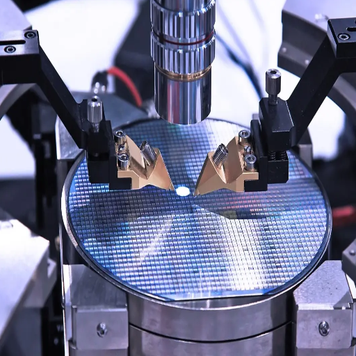
Cutting a silicon carbide (SiC) wafer is an imperative and delicate operation when producing semiconductor structures. It helps to safeguard the strong building of the material with as little wastage as possible. This is basically mechanical sawing or laser cutting, designed, however, to cope with the SiC hardness and brittleness. Cutting speed, blade material, and cooling factors are among the key issues that need to be addressed while cutting. SiC wafer cutting performed with the help of these parameters aids in achieving the desired dimensions and surface finish of a wafer that is generally quite important for other processes like polishing and fabrication of devices.
Overview of SiC (Silicon Carbide) Material Properties
Silicon Carbide (SiC), being a compound recognized by a wide range of properties in its physical chemistry, does not escape the attention of researchers in terms of new possibilities in electronic and industrial domains. For instance, SiC is characterized by a large bandgap of about 3.2 eV and is capable of operating at very high temperatures, voltages, and frequency ranges. It possesses high thermal conductivity (around 3.7 W/cm·K) and therefore good heat dissipation properties, which are important for power electronics. SiC wafers, on the other hand, are inherently hard with a hardness value of 9 in the Mohs scale and high tensile strength; thus, they have high wear and corrosion resistance.
In addition, the chemical stability of SiC is notably high even in the most hazardous conditions, thanks to its low resistance against oxidation and other types of chemical degradation. And in this context of energy-efficient devices, the low dielectric constant and the high electric field strength contribute to the improved performance of SiC-based systems. The advancement and application of these features have encouraged industries such as electric automobiles, renewable sources of energy, air transport, and communications to embrace the material, and as a result, SiC has become an integral component in future technology.
| Property | Value / Description | Significance |
|---|---|---|
| Bandgap | ~3.2 eV | Enables high-temperature & high-voltage operation |
| Thermal Conductivity | ~3.7 W/cm·K | Superior heat dissipation for power electronics |
| Mohs Hardness | 9 – 9.2 | High wear & corrosion resistance; demands diamond tools |
| Chemical Stability | Very High | Low oxidation & chemical degradation in harsh conditions |
| Electric Field Strength | High | Improved performance in energy-efficient devices |
Importance of Precision in Wafer Cutting Processes
Ensuring the quality and performance of semiconductor devices demands a high level of precision in the silicon wafer cutting processes. Cutting to high precision levels leads to efficient material use and production within tolerance limits of micro-cracks or chipping, and most importantly, achieving consistency in the wafers’ dimensions, since it is important in the processes that follow. There have been improvements in the cutting techniques, such as diamond wire sawing and laser cutting, and this allows attainment of higher levels of both accuracy and efficiency, hence the wafers produced are thinner and more uniform with almost no damage. Such developments have a direct impact on the performance of the devices and the cost of manufacture, which explains why precision is of utmost importance in the semiconductor technology progress.
Applications of SiC Wafers in High-Power Electronics and Other Industries
It’s no wonder that Silicon Carbide (SiC) wafers play a key role in the development of high-power electronic devices – this is mainly attributed to the outstanding electrical and thermal characteristic features exhibited by the material. Examples of SiC components include MOSFETs and Schottky diodes, which have a variety of high-demand applications that require high efficiency and reliability. The utilization of SiC in electric vehicles (EVs) by the automotive industry allows the powertrain to be compact, has fewer losses in the system, and permits a longer distance to be covered. In the same way, energy renewable technologies, i.e., photovoltaic and wind power forms, have SiC applications in order to improve the efficiency in energy transformation and reduce wastage of the power generated.
Apart from the above applications, SiC is additionally applicable in most of the industries where high temperatures or high voltages exist. Exceptionally high thermal stability and thermal conductivity make it a perfect material for power-effective applications such as servers, pumps, and equipment. In compact and rugged systems, the aerospace and defense sectors install SiC materials for devices functional in hostile environments. The wide range of applications points to the significance of the effect of sic wafer cutting technologies in electronics and energy-potential improvements.
🚗
Automotive / EV
Compact powertrain, reduced losses, extended range
⚡
Renewable Energy
Photovoltaic & wind power efficiency improvement
✈️
Aerospace & Defense
Compact, rugged systems for hostile environments
🖥️
Industrial Power
Servers, pumps & high-temperature equipment
Key Challenges in SiC Wafer Cutting
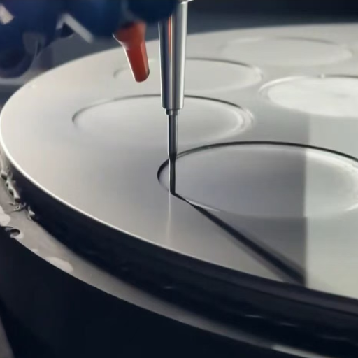
SiC wafer cutting has numerous constraints that present themselves because of the hardness and brittleness of the SiC material. Considering its high mechanical hardness of 9.2 on the Mohs scale, the diamond tool wears too fast, and such cutting tools are supposed to be made of a diamond coat, which, however, adds to the production cost. The brittle nature of SiC also increases the likelihood of microcracks or chipping while performing the cutting itself, thus affecting the integrity of the wafer and the yield. It is also hard to cut due to the generation of heat during the process, leading to difficulties, particularly because SiC is a good thermal conductor and therefore heat needs to be evacuated to avoid this problem. Thus, high-quality wafer manufacturing is only attainable through the optimization of cutting elements and procedures, incorporating tool material selection and appropriate cooling measures.
⚠ Hardness Challenge
Diamond tools wear rapidly due to SiC’s 9.2 Mohs hardness, significantly increasing production cost.
⚠ Brittleness Risk
Brittle nature increases likelihood of microcracks and chipping, affecting wafer integrity and yield.
⚠ Heat Generation
Cutting generates significant heat that must be managed to prevent thermal stress and material damage.
⚠ Surface Damage
Edge chipping and surface damage threaten the strength and functional reliability of SiC components.
Hardness and Brittleness of SiC Material
One of the most resistant materials in nature and industry is Silicon carbide (SiC), whose hardness is surpassed only by a few surrounding scales of the Mohs scale, about 9.2. The tremendous hardness of silicon carbide is due to its crystal structure, where silicon and carbon are strongly bonded to each other. This feature of the cutting tool material includes both advantages and limitations, among which is the inability of excessive plastic deformation during loading. This nature of the material gave rise to the concept of rupture-induced stress since there are low active slips and a greater tendency towards advancement of fracture under stress. Therefore, SiC wafer cutting manufacturing processes call for new advanced processing methods because the traditional ones will lead to unwanted fracture with no indulgence in the wafer’s dimensions.
Heat Generation and Potential Thermal Stress
Cutting of silicon carbide (SiC) wafers in fabrication turns out to be a source of heat, as well as high-precision machining in both performance and working devices. However, this heat can be dissipated effectively due to the relatively high thermal conductivity of SiC compared to other semiconductors. Local rise in temperature is, however, a possibility, and it can precipitate heat stress. Thermal stresses occur in a material due to a lack of uniformity in thermally induced expansions and contractions. These stresses may lead to damage in the form of cracks, changes in microstructure, or even device breakdown. To avoid these undesirable situations, proper thermal management includes sophisticated liquid cooling solutions or non-essential TIMs (Thermal Interface Materials) – one of the fundamental measures needed at all stages of device construction and operation.
Surface Damage and Edge Chipping Risks During Cutting
Since silicon carbide (SiC) is a hard, brittle material, the risk of surface damage and edge chipping when cutting the material is very high. These problems are mainly caused by the use of conventional machining techniques that place heavy mechanical stresses on the material. Such edge chipping is especially important because it affects the strength and functional reliability of SiC components. In order to avoid these concerns, processes such as precision diamond sawing, laser cutting, and high-precision wire EDM (electrical discharge machining) were introduced in order to minimize the material subtraction process. Moreover, too high or too low cutting actions are avoided, and heat and cooling parameters are controlled in order to reduce thermal and mechanical stress, and surface and edge damage to the material is minimized as much as possible. The use of these sophisticated techniques offers protection of SiC-based devices for some of the applications suggested.
Essential Equipment and Tools for SiC Wafer Cutting

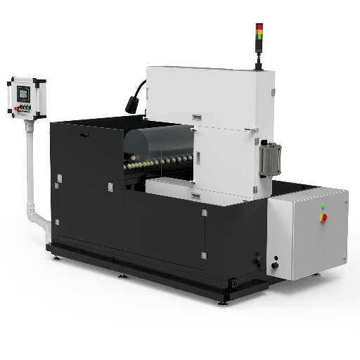
There are many tools and facilities required in the SiC wafer cutting process in order to ensure it is done effectively and accurately. Utilizing a diamond wire saw, which is effective in cutting through the material without excessive loss, is almost universal when working with SiC because of its hardness. Moreover, precision grinding machines with diamond abrasives are another MUST-have when preparing cut surfaces. Also, such high-energy lasers are instrumental in laser systems because they enable contactless operations with materials. Another good method of performing neat cutting would be those water-jet systems enhanced with abrasive particles. Among the support systems available, ultrasonic washers help clean the wafers, which will help avoid contamination during the next steps of manufacturing. All these tools aid in increasing precision, reducing time, and improving the output in the processing of the SiC wafers.
Essential Equipment Overview
- 1
Diamond Wire Saw — Effective for cutting through hard SiC material with minimal material loss
- 2
Precision Grinding Machines — With diamond abrasives for preparing cut surfaces to the required finish
- 3
High-Energy Laser Systems — Enable contactless cutting with high precision and minimal thermal damage
- 4
Abrasive Water-Jet Systems — Enhanced with abrasive particles for precise material removal
- 5
Ultrasonic Washers — Prevent contamination between manufacturing stages by thoroughly cleaning wafers
Types of Dicing Saws and Diamond Blades
Various kinds of diamond blades and dicing saws are used in silicon wafer cutting due to their accurate and effective performance. These dicing saws are broadly classified into manual, semi-automatic, and fully automatic systems. Fully automatic dicing saws are most preferred in the semiconductor industry as they can process a large number of wafers, have precise alignment ready-made, and can be used to deal with ultra-thin wafers with close to no damage.
Diamond blades used in dicing operations differ in construction, depending on what is being shaped, like Silicon Carbide (SiC) wafers or some other stuff. All diamond blade types have one of the following: resin-bonded, metal-bonded, or electroplated binders. For soft materials that are prone to chipping, resin-bonded blades can be used, while for hard materials like SiC, metal-bonded blades are more useful as they do not suffer wear easily. These blades are best suited for applications with strict precision demands and where the width of the incision is very important, which is why such systems are good in semiconductor or mechatronics operations. Upon choosing a combination of a particular saw and an appropriate diamond blade cutting element, the above mentioned problems do not exist, i.e., there is no wastage of materials due to over-cutting and early breakage, and this equipment lasts longer with the current advanced cutting of the wafers.
| Blade Type | Best For | SiC Suitability |
|---|---|---|
| Resin-Bonded | Soft materials prone to chipping | Not Recommended |
| Metal-Bonded | Hard materials like SiC, minimal wear | Recommended |
| Electroplated | Strict precision demands, narrow kerf width | Context-Dependent |
Role of Laser-Cutting Technology
Laser-cutting technology is now considered an essential step in the development of modern methods of production, especially when it comes to the semiconductor and microelectronics industries. This technology, which is a non-contact technique, encompasses the application of focused laser rays that cut, drill, or engrave materials at high precision without applying any unwanted forces, thereby best suited for enhancing the processes of materials that are sensitive, such as silicon, glass, and ceramics. Concise utilization of the short pulse or very short pulsed lasers results in fast output of the processes without any harsh edges or much heat affected, as in conventional methods.
In addition, laser cutting works for highly complex shapes as well as very precise microfabrication (for example, down to micrometers). It is applicable in almost every fabrication method, such as SiC wafer cutting, making via holes, surface texturing, etc., for miniaturized components and advanced electronics. The approach also allows efficient use of materials with minimal waste, which is one of the main concerns of the current modern manufacturing methods. In the event that laser cutting is employed with the help of automation, efficiency and consistency levels are increased due to the fact that it is an invaluable tool that can be used in precision engineering and high-performance manufacturing facilities.
Importance of Coolant Systems and Blade Dressing Tools
Elements such as coolant systems and blade dressers are essential in making sure that the cut and grind operations are productive, long-lasting, and accurate. The presence of coolant systems is critical when performing tasks that involve machining, such as SiC wafer cutting, ensuring that any heat produced does not cause thermal deformation of the tool or the workpiece. They are also useful in cleaning up the chips and lubricating the surface to reduce friction and imperfections that result in roughness. Tool life is importantly enhanced by the application of correct coolant, owing to the fact that the coolant achieves the objective of dimension correctness and prevents damage to the workpiece.
Abrasive surface of cutting and grinding wheels should also be dressed from time to time to restore their performance. This is because the wheel’s surface can be clogged up and fail to cut, so dressing gets rid of the padding to bring fine abrasive particles into the surface for even cutting and better performance. Good blade dressing minimizes the danger of disc wear and prolongs the use of advanced tools. In no other way can the precision, the economy, and high quality in manufacturing of a technological level without these two technologies.
SiC Wafer Cutting Process Parameters
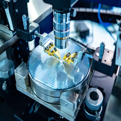
Several technologies underpin the SiC wafer cutting logistical infrastructure, but on the operational level, only a few parameters define the effectiveness and precision of cuts.
Key Process Parameters
- 01
Cutting Speed (Feed Rate)
Cutting tools are moved at a certain speed over the SiC wafer to cut it. The produced surface and the rate of production also depend on this speed. Very high cutting speeds result in less precision, and very low speeds result in high precision but a lower production rate. - 02
Abrasive Grit Size
The amount of abrasion for cutting and polishing is also based on abrasive size. The finer the abrasive, the smoother the surface but the slower the cutting process; the coarser the abrasive, the faster the cutting process. - 03
Saw Blade Tension
The tension of the blade should be high enough so that it enhances cutting performance by preventing vibrations, which may lead to chipping or crack propagation. - 04
Coolant Flow Rate
Cooling the process sufficiently rejects excess heat, eliminates wear on the tool, causes less choking of the cut surfaces, and cleans the surfaces by removing the waste. - 05
Depth of Cut (DOC)
This term refers to the thickness of the workpiece being cut in a single pass. Setting this parameter properly prevents overheating and excess stress in the wafer.
These parameters should be kept in a way that optimizes results in the end, maximizing accuracy, minimizing material waste, and striving for longer usage of the tool.
| Parameter | Low Setting Effect | High Setting Effect |
|---|---|---|
| Cutting Speed | High precision, lower throughput | Lower precision, faster production |
| Abrasive Grit Size | Smoother surface, slower cutting | Faster cutting, rougher surface |
| Blade Tension | Increased vibration, chipping risk | Reduced vibration, stable cuts |
| Coolant Flow Rate | Heat buildup, tool wear | Effective cooling, cleaner cuts |
| Depth of Cut (DOC) | More passes, less stress per pass | Fewer passes, risk of overheating |
Optimal Feed Rate and Cutting Speed
When it comes to the usage of CNC machines, cutting speeds and feed rates are important for machining processes because they determine the effectiveness, precision, and time of tools. Feed rate describes the length of advancement of the cutting tool or the workpiece per every revolution of the spindle and is expressed in units that may include inches per minute (IPM). Determining the ideal feed rate takes into consideration the cutting force, wear of the tools, materials, and other factors, so as to limit cutter breakdown and surface defacing.
The Cutting speed is often expressed in terms of surface milling feet per minute (SFM) or meters/minute (m/min). It is affected by the hardness of the workpiece material, geometry of the hydraulic tool, application of coolant, etc., and has to be accurately determined to prevent heat generation and ensure effective cutting of the SiC wafer.
Manufacturers focus on ensuring that firms regulate the standards, which means that for characteristics dependent on a material and the tools, they invest in the standards by providing reference data of various tool manufacturers’ charts in order to apply the recommended levels for a certain material and tool concerned. Exactness is inescapable in aggressive machining spheres since it is the scientific approach in combination with its operand practices that leads to shorter enhanced cycle times, surface integrity, and extended tooling lifespan.
Blade Wear Monitoring and Maintenance Strategies
Proper strategies for blade wear monitoring and maintenance are important in enhancing machining output and extending the operational life of the blades. The strategies sometimes involve technologies that include items like sensors, which are installed on large tools for real-time activity, and machine learning techniques that depend on changes in the cutting conditions and behavior of the one-way wear patterns. Visual assessment helps confirm blade conditions more meaningfully in combination with measuring devices e.g. microscope and profilometer. Strategies tend to take a wider approach, which consists of re-sharpening, for example, cleaning the blades to avoid the build-up of substance, and also following the operating instructions supplied by the manufacturers. Predictive maintenance, which can be accomplished through the use of data analysis, is likewise versatile enough to begin to detect wear-induced failures, which interrupt productive activities and ensure efficient deployment of resources in demanding production industries.
Coolant Flow Rate and Temperature Control Considerations
It is important to maintain adequate flow rates and temperatures of the coolant to perform the machining process effectively and to increase the life of the cutting tool. The coolant flow rates should be so high that the heat generated due to cutting or grinding might be effectively removed; otherwise, thermal stresses would be created within the tools, and these tools would break. Flow rates are normally determined by the kind of material processed, the speed of cutting, and the geometry of the tool so that the cutting zone is lubricated and cooled evenly. From the same perspective, an accurate temperature range of operation prevents the boiling and extreme viscosity changes of the coolant to a level that adversely affects the processes. These parameters, with the help of enhanced sensor applications as well as automation, are continuously controlled in order to keep tools and workpieces intact, as far as avoiding their thermal distortion and process control as much as possible.
Best Practices for Improving Cut Quality and Yield
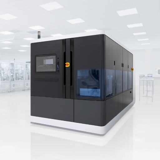
Various basic measures and tools are applicable for cutting, where dimensional accuracy is necessary for SiC wafer cutting. To improve the performance of the cutting tools, one will only use the appropriate tools and machinery as dictated by the current material chosen, use an optimal coating and tool design, and ensure sharpening laps within productivity limits. In addition, mechanical adjustments must be secured or kept to minimal intervention. This is to ensure that the machine does not come out of calibration, affecting the actual and desired position. To curb temperature rise, particularly if the energy usage is bound to be extremely high, high-performance lubricants and coolants should be used for basic machining operations. By integrating the usage of monitoring systems like vibration sensors or temperature sensors, the quality is controlled within a certain range as warnings/alerts are received early enough and adjustments are made instantly. But most importantly, it is necessary to adjust the feed rate, cutting speed, and cutting depth, which are tested or simulated before the actual work in machining the workpiece. SiC wafer cutting and optimization of cutting parameters can improve yields effectively without sacrificing the life of the tool.
✓ Best Practice Checklist
- ✓ Use appropriate tools and machinery as dictated by the material being processed
- ✓ Apply optimal coating and tool design with timely sharpening within productivity limits
- ✓ Keep mechanical adjustments secured and minimal to preserve machine calibration
- ✓ Use high-performance lubricants and coolants to curb temperature rise during machining
- ✓ Integrate vibration and temperature sensors for real-time quality monitoring
- ✓ Test or simulate feed rate, cutting speed, and depth adjustments before actual machining
Strategies to Reduce Edge Defects and Microcracks
Effective strategies that should be employed in any attempt to prevent edge defects and microcracks include: meticulous machining, optimal choice of machinery, and the right set of process parameters. However, it is important to understand the basic concept of leverage, which involves the use of highly specified cutting tools equipped with appropriate (diamond or ceramic) coatings for better cuts and decreased wear. Proper lubrication and coolant application provide an effective solution for generating less heat and reducing in-process wear, which otherwise causes surface stress and subsequent cracking. In some cases, laser-assisted manufacturing or ultrasonic vibration techniques, however, can reduce the mechanical stress and consequently increase the accuracy. For the purpose of minimizing irregularities, which could contribute to defects, the tool must be maintained at the desired state through the use of preventive maintenance and frequent calibration. Finally, control of environmental conditions, including vibration isolation of machinery and regulation of the temperature within the working area, mitigates the generation of microcracks and edge defects in the course of production.
Defect Reduction Strategy Guide
- Use highly specified cutting tools with diamond or ceramic coatings for better cuts and decreased wear.
- Apply proper lubrication and coolant to generate less heat and reduce in-process wear that causes surface stress and cracking.
- Consider laser-assisted manufacturing or ultrasonic vibration techniques to reduce mechanical stress and increase accuracy.
- Implement preventive maintenance and frequent calibration to keep tools at the desired state and minimize irregularities.
- Control environmental conditions — vibration isolation of machinery and regulation of working area temperature — to mitigate microcrack generation.
Techniques for Maximizing Wafer Utilization Efficiency
Minimizing wastage of silicon wafers in design is a primary objective, for taking care of arranging everything in such a manner that there is very little waste of material. This means using mathematical models and working out the exact quantities for the die and users’ areas. Also ensuring the use of kerf-free or kerf reduction where applicable. There is a consistent review of the yield rate, and inefficiencies can be easily realized for timely corrective action. More importantly, these strategies are implemented with tight process control to eliminate the inefficiency that arises in every cycle of the SiC wafer cutting maximization effort.
Post-Cutting Damage Inspection and Correction Procedures
It is vital that all dicing wafers are inspected for post-cut defects so as to maintain the integrity of the materials. Such a procedure consists of special microscopes or scanning electron microscopes/scanning microscopes to look for microcracks, chipped axial corners, or contamination on the surfaces after the silicon wafer cutting takes place. Employment of automated image acquisition mechanisms is a common practice to enhance accuracy while limiting the effect of the operator.
After some damage is discovered, chemical procedures such as etching and polishing are used with respect to surface defects and stress concentration at the wafer border circumference. In case of edge defects such as chipping, a laser annealing or beam sharpening might be carried out in order to restore the structural state of the disk. In addition to the latter, the wafer is often cleansed with the help of ultrasonic or megasonic processes, which take out different particles and contaminants impeding the operation of a device. These inspection and correction procedures help in ensuring the quality of wafers for further applications. Essentials of the zones included in curved SiC wafer cutting operations are included in inspection and calibration processes.
| Step | Method | Defects Targeted |
|---|---|---|
| 1. Visual Inspection | Microscope / SEM / Automated imaging | Microcracks, chipping, contamination |
| 2. Surface Correction | Chemical etching & polishing | Surface defects, stress concentration |
| 3. Edge Restoration | Laser annealing / beam sharpening | Edge chipping, structural damage |
| 4. Final Cleaning | Ultrasonic / megasonic cleaning | Particle contamination, impurities |
Reference Sources
“Dual Laser Beam Asynchronous Dicing of 4H-SiC Wafer”
This study introduced a novel dual laser beam asynchronous dicing (DBAD) method to enhance the cutting quality of SiC wafers. The method uses a pulsed laser to improve precision and reduce defects.
“Study on the Impact of the Cutting Process of Wire Saw on SiC Wafers”
The study explored the effects of cutting fluid and wire saw parameters on the cutting rate and surface quality of SiC wafers. It highlighted the importance of optimizing cutting conditions.
This review discussed the limitations of traditional wafer cutting methods and the advantages of ductile cutting technology for silicon wafers, with implications for SiC wafers.
Frequently Asked Questions (FAQs)
How does laser technology contribute to the cutting of silicon carbide wafers?
Laser technology, more so the ultrafast and femtosecond laser processing, offers a non-contact slicing method for silicon carbide wafers, which mitigates the mechanical stress on the high hardness and brittleness of the silicon carbide crystal. The use of laser beam and pulse laser techniques can be done to form modified layers specifically in cutting-locked pattern in 4H-SiC wafer using picosecond pr femtosecond laser pulses, thus reducing kerf loss as opposed to the traditional cutting methods and reducing the necessity for further/different grinding and polishing of end products to meet the surface finish desired.
In wafer slicing for SiC, what should be done when trying to use a semiconductor dicing saw to slice below 100 μm SiC wafers?
Femtosecond and picosecond laser technology and ultra-fast lasers are terms used to describe laser technology that can create very short laser beams. Under laser induced zero thermal effects, it is possible to achieve very precise laser machining of silicon carbide wafers without any heat affection accompanied by the formation of a modified layer. This method of ultra-fast pulse laser application makes it possible to enhance wafer surface properties, reduce surface roughness, and advance the high-precision cutting process necessary for applications in power electronics, semiconductors, and advanced materials like semi-insulating SiC substrates.
When cutting the SIC wafer, which of the two methods will enable achieving better surface properties?
Laser beam isolation may be considered as a variant of laser cutting technology, in which the irradiation is carried out through a series of impulse ultrashort (femtosecond) or short (picosecond) pulses and results in close modification of the structure of the material. It has been found that this type of interaction hardly results in a lot of accuracy loss, chipping or damage, and minimizes finish post-work significantly. There are benefits in the application of diamond wire cutting as a more conventional precision cutting technology, particularly in terms of glass and silicon wafers. Suitable applications for wire cutting depend on the dimensions calculate of sliced off the ingot, the cost of the material, its size, and the feature that would be found in a semiconductor they are manufacturing.
Stealth dicing vs. laser cutting. Who is going to win the silicon carbide fight?
Stealth dicing and laser scribing are both methods that use a form of focused energy from lasers, but in different ways. In the case of stealth dicing, for instance, the energy causes a series of micro-cracks in the material, which are then expanded to encourage the material to break off in a tear, while in the case of direct laser irradiation or ultra-fast cutting, the energy causes the formation of such an altered layer that the slices are efficiently plucked. However, stealth dicing may be virtually impossible to accomplish in cases involving silicon carbide because of its high bon hardness and hence the need to adjust this process slightly; the use of ultrafast laser cutting techniques though provides much more accurate separation with lower mechanical stresses, which is as good as possible to tell, but both of these will most likely entail slicing and grinding and polishing to certain final surface requirements highlighting in power device production for wafers.
What kind of post-cutting operations are going to be involved after the active slicing of the SiC wafers?
After dicing – using any of the laser method, diamond wire, conventional cutting – silicon carbide wafers always go through the removal of the reprocessed layer from the surface by the grinding, lapping, and polishing to achieve a contamination-free and flaw-free wafer surface for further semiconductor manufacturing process. Subsequent stages of grinding and polishing are process steps without which the fabrication of ICs, power conversion applications, and implementation in new vehicles of the high-performance, high-temperature photonic devices and SiC power devices are impossible.
Related Posts

Trending Blogs

![Polysilicon Material: Properties, Grades & Uses [Guide]](https://wiresawcutter.com/wp-content/uploads/2026/08/polysilicon-material-featured-150x150.webp)