Get in touch with DONGHE Company

By the Shanghai Donghe Science and Technology Co., Ltd. technical team · Updated June 2026
The diced wafer process is the back-end step where a finished semiconductor wafer is cut into hundreds or thousands of individual dies, each one a working chip ready for packaging. It’s also called die singulation, and it sits at the very end of the fab flow: an ingot is sliced into wafers, the wafers are patterned and thinned, and only then are they diced. This guide to wafer dicing walks the full sequence station by station, compares the four main dicing methods with real kerf and feed-rate numbers, and shows where most yield gets lost.
The diced wafer process separates a finished wafer into individual dies, almost always as the last operation before packaging. Engineers pick from four methods, blade, laser, plasma, and stealth dicing, that differ mainly in kerf width (from roughly 20-40 µm down to near-zero) and in how much they weaken the die. Method choice is driven by wafer thickness, material hardness, street-width budget, and the die break strength the package need.
Quick Specs, Typical 200 mm Silicon Blade Dicing
| Blade kerf (≈ blade width) | 20-40 µm |
| Spindle speed | 15,000-30,000 rpm (up to 60,000) |
| Feed rate | 1-5 mm/s (test) → 25-75 mm/s (production) |
| Diamond grit size | 2-4 µm (fine) to 6-8 µm (hard materials) |
| Cut depth per pass | ≤500 µm |
| Dicing tape | UV-release (thin die) or blue/non-UV (standard) |
| Target die break strength | ~500-1,000 MPa (silicon) |
Values vary by material, die size, and machine. Sources: University of Michigan LNF process wiki and published dicing studies (full source list at the end of this guide).
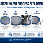
What Is the Diced Wafer Process? (Die Singulation Explained)

Die singulation is the operation that turn one patterned wafer into many separate chips. After lithography and etching build the circuits, and after the wafer is thinned by back-grinding, the dies still sit in a single sheet of silicon connected by narrow blank lanes called streets (or scribe lines). Dicing cuts along those streets so each die can be picked and packaged.
It helps to place dicing in the larger flow, because two cutting steps get confused. First, a wire saw slices the crystal ingot into raw wafersthat’s slicing. Much later, after the wafer is fully fabricated, dicing singulates it into dies. Slicing and dicing happen at opposite ends of the process and use different machines: the upstream slicing cut is handled by a silicon wafer cutting wire saw, while dicing uses a dicing saw, laser, or plasma chamber.
Remember the order this way:
- Ingot → slice (wire saw) → bare wafer
- Bare wafer → fabrication (the litho-and-etch manufacturing process) → patterned wafer
- Patterned wafer → back-grind / thin → dice → pick → package
Within the larger semiconductor manufacturing process, dicing is the bridge between front-end fabrication and back-end assembly: it ends the fabrication process on the wafer and begins the assembly process on the die. Because it’s the one mechanical-separation step in an otherwise additive process in semiconductor manufacturing, dicing carries outsized yield risk. Most production volume is silicon wafer dicing, and the dicing of silicon wafers sets the baseline recipes that other materials are tuned against, a single wafer, a 300 mm Si wafer, can yield thousands of separate wafer die from one entire wafer. An older alternative, wafer scribing, scores a shallow line so the wafer breaks along crystal planes; it’s fast and stress-free but limited to straight cleavage directions.
Where slicing is judged on flatness and kerf loss across a whole boule, dicing is judged on chip-free die edges and surviving break strength. Both steps share one root challenge, they cut hard, brittle crystals, which is why the same materials show up in both worlds: silicon, silicon carbide, and sapphire. If you’re new to the substrate side, our overview of the main types of semiconductor wafers gives the background that dicing assumes.
The Wafer Dicing Process, Step by Step

A production dicing line is a sequence of seven stations, and each one control a different failure mode. We call this end-to-end flow the Mount-to-Pick Dicing Sequence: every die has to survive all seven stations to ship, so the weakest station set your yield.
| # | Station | Purpose | Key control / failure mode |
|---|---|---|---|
| 1 | Back-grind / thinning prep | Reduce wafer to final thickness | Residual back-side damage seeds cracks later |
| 2 | Tape & frame mounting | Bond wafer to dicing tape on a ring frame | Air bubbles or weak adhesion → die fly-off |
| 3 | Alignment / teach | Machine recognizes the streets | Misalignment cuts into device structures |
| 4 | Cutting | Saw, laser, or plasma separates the dies | Chipping, kerf width, blade wear |
| 5 | Rinse & clean | Flush debris with DI water | Residue and particles fail later bonding |
| 6 | Inspection | Measure chipping and kerf | Out-of-spec chips disqualify dies |
| 7 | UV-cure, expand & pick | Weaken tape, spread dies, lift them off | Pick force cracks thin die |
Station logic compiled from the University of Michigan LNF dicing wiki and equipment-maker process notes.
A few stations deserve a closer look. Alignment (station 3) teaches the saw to ensure precision over every street, the blank dicing lanes between dies, so each cut track the lane and never clips a device structure. Station 2 is the tape mounting process: the wafer is bonded to dicing tape stretched across a metal ring frame; the tape hold the wafer flat while the frame is what the saw chuck actually grips. Dicing tape must hold every die in place during the cut, then let go cleanly afterward, which is why UV-release tape is used for fragile thin dies: a dose of ultraviolet light drops its adhesion so dies lift off without stress. During cutting (station 4), DI water is sprayed onto a spinning blade to flush debris and carry away friction heat, following the spindle-speed, feed, and exposure rules documented by the University of Michigan Lurie Nanofabrication Facility dicing reference. At the final station, the tape is expanded to open gaps between dies so a pick-and-place tool can lift each one.
How long does a typical wafer dicing cycle take for a 200 mm silicon wafer?
There’s no single published cycle time, because it depends on die size, cut count, and method. For blade dicing a 200 mm silicon wafer cut into 5 mm dies, expect roughly 5 minutes of pure cutting, but tens of minutes end-to-end once alignment, indexing, cleaning, and inspection are added in.
As a worked estimate, about 40 cut lines per axis at a 50 mm/s feed give 40 × 2 × 4 s ≈ 320 seconds of cutting. Plasma dicing breaks this pattern: it etches all streets in parallel, so its time advantage grows as die count rises.
The 4 Main Wafer Dicing Methods

Four methods dominate the diced wafer process. These different dicing methods split into two families: contact methods that touch the wafer, mechanical dicing, also called saw dicing, using diamond dicing blades spun on a saw blade spindle, and non-contact methods (laser, plasma, and stealth). They differ most in kerf width, the material a cut consumes, and in how much they weaken the resulting die. Blade dicing grinds a physical groove; laser dicing vaporizes one; plasma dicing chemically etches all streets at once; and stealth dicing leaves the wafer surface almost untouched, forming a buried fracture line that you later pull apart.
| Method | Mechanism | Typical kerf | Throughput | Die strength | Best fit |
|---|---|---|---|---|---|
| Blade (mechanical) | Diamond disc grinds the street | 20-40 µm | Serial; 25-75 mm/s | Lowest (chip/microcrack) | Standard, thicker silicon; cost-sensitive |
| Laser ablation | Pulsed beam vaporizes the street | Single-digit µm + heat zone | Serial, often multi-pass | Moderate; debris/HAZ | Thin, fragile, narrow streets |
| Plasma (DRIE) | Fluorine plasma etches all streets | ~10-20 µm | Parallel (all at once) | Highest as-diced | Thin <50 µm, MEMS, hybrid bonding |
| Stealth (IR laser) | Buried modified layer, then expand | ~Kerf-free | Fast, dry, no slurry | High; competitive with plasma | Ultra-thin silicon, kerf-critical |
Kerf and plasma temperature data from published dicing literature and process wikis; stealth dicing mechanism per peer-reviewed analysis (full source list at the end of this guide).
Plasma dicing runs cold, the chemical etch keep the wafer below about 60 °C, and because it cuts every street in one parallel pass it scales well when a wafer holds tens of thousands of small dies. Stealth dicing, originated by Hamamatsu, focuses an infrared laser inside the silicon to create a subsurface modified zone, the internal-modification mechanism claimed in USPTO patent US 11,646,228 B2; the wafer is then stretched on its tape until it cleaves along those zones, removing no material and producing almost no debris. That kerf-free behavior is why stealth and plasma have largely taken over the thin-die and advanced-packaging segment.
How to Choose a Dicing Method

Method selection comes down to a three-way tension we call The Dicing-Method Tradeoff Triangle: kerf loss, throughput, and die break strength. You can usually win on two of these and must give ground on the third, so the right method is the one whose weak axis matters least for your device and package.
Selection tracks wafer thickness and material hardness more than brand preference, the same variables that fix blade and feed settings in fab process references like the University of Michigan LNF dicing guide. A blade is fast and cheap but eats the widest kerf and inflicts the most edge damage. Plasma gives the narrowest kerf and strongest dies but cuts in parallel only after a costly chamber and gas-handling investment. Stealth removes no material and runs dry, but its throughput is sensitive to thickness and street layout.
Conditional method selector
- Thin die under ~100 µm, strength is critical → plasma or stealth dicing.
- Thick standard silicon, budget-driven, generous streets → blade dicing.
- Very narrow streets or maximum dies-per-wafer → plasma (kerf ~10-20 µm) or stealth (kerf-free).
- Hard or brittle compounds (SiC, GaAs) where blade wear is severe → laser or stealth.
- MEMS, sensors, or HBM stacks for hybrid bonding → plasma.
One myth is worth correcting here. Vendor literature often states that plasma dicing always gives higher die strength than stealth dicing. The peer-reviewed picture is more careful: a widely cited review of singulation technologies notes that post-dicing strength enhancement has become a complement to most methods, meaning the final strength depend heavily on post-processing, not the cutting method alone. Quoted strength ranges for the two methods overlap. Plasma usually produces the highest as-diced strength because it leaves no mechanical or thermal damage layer, but stealth is competitive on thin silicon and can close the gap after edge-strengthening steps. Treat strength as a tradeoff to engineer, not a contest one method always win.
Whether you dice in-house or send wafers to precision wafer dicing services, write down your dicing requirements before you commit to a method: target die thickness, street width, minimum die strength, and volume. Shops offering high-precision wafer dicing services map those process requirements onto a specific wafer dicing technique and quote against them. The most common wafer dicing challenges, edge chipping, blade wear, and thin-die handling, get easier to solve when your dicing needs are written as numbers rather than adjectives, and the right dicing solutions usually fall out of that one-page spec.
Dicing Saws, Blades, Tape & Consumables

A blade-dicing setup is a system of matched consumables, and small choices here drive most of the chipping you see at inspection. Each blade is a thin diamond-abrasive disc, usually 20-40 µm thick, thinner blades cut a narrower kerf but bend and break more easily. Diamond grit size trades quality against speed: 2-4 µm grit produces smoother, lower-microcrack edges but cuts slowly, while 6-8 µm grit is reserved for hard materials like silicon carbide. The bond holding those diamonds matters too, nickel bonds retain grit firmly and last long, resin bonds cut with lower force and less chipping but wear faster, and sintered-metal bonds suit the hardest substrates.
📐 Engineering Note — Blade exposure & coolant
Set blade exposure greater than the cut depth plus about 25 µm of over-cut into the tape, plus a safety margin of at least 100 µm so debris and slurry can exit the kerf. Too little exposure traps debris and chips the die. Run DI water as coolant rather than tap water, its high resistivity prevent ionic contamination and electrostatic discharge, and surfactant or antistatic additives help flush fine particles. A hubless blade with a large flange and short exposure keeps side runout low for narrow 12-25 µm kerfs.
Tape is the other half of the system. UV-release tape is the default for thin dies because its adhesion can be switched off on demand; blue non-UV tape is fine for standard silicon. For standard silicon, blue non-UV dicing tape is the economical default; UV-release tape is reserved for thin or fragile die. For wafers under 100 µm, a dual-layer tape, one adhesion layer plus one stress-absorbing layer, keeps the die from flexing and cracking during the cut. High-volume fabs often run a dual dicing saw with two spindles cutting in parallel to lift throughput, though most mechanical dicing saws share the blade, flange, and coolant architecture described here. If you’re also handling the abrasive side of hard-material processing, our note on silicon carbide as an abrasive explains why grit form and friability change how aggressively a tool cut.
Material-Specific Dicing: Si, SiC, GaAs, Glass & Sapphire

Dicing parameters aren’t universal, they shift with the hardness and brittleness of the substrate. Silicon is the mature baseline. Silicon carbide and sapphire are extremely hard and wear blades quickly, SiC’s fracture toughness of roughly 1.4-1.8 MPa·m¹ᐟ² (peer-reviewed measurement, PMC) is why its dicing push toward laser and stealth methods. Gallium arsenide is soft but very brittle and produces toxic dust. Use the table below as a starting point that you tune to your own machine and die layout.
| Material | Class / character | Feed | Spindle | Watch for |
|---|---|---|---|---|
| Silicon | Moderate brittleness | 25-75 mm/s | 30-50 krpm | Back-side chip on thin die |
| Silicon carbide (SiC) | Extremely hard | 20-40 mm/s | 25-35 krpm | Rapid blade wear, heat |
| Gallium arsenide (GaAs) | Brittle, toxic dust | 10-25 mm/s | 40-50 krpm | Microcracks, dust control |
| Sapphire | Very hard, brittle | Low | — | Catastrophic fracture risk |
| Glass / LiNbO₃ | Subsurface-crack prone | Low | — | Coolant flow, mount stress |
| Indium phosphide (InP) | Soft, cleaves on planes | 10-25 mm/s | 30-40 krpm | Cleavage cracks, chipping |
| Gallium nitride on sapphire (GaN) | Hard epi on hard substrate | Low (laser/stealth) | — | Epi film delamination |
| Germanium (Ge) | Soft, brittle | 15-40 mm/s | 30-45 krpm | Edge chipping, IR handling |
| Quartz / fused silica | Hard, transparent, brittle | Low | — | Subsurface cracks |
Material matrix from equipment-maker guidance; SiC fracture toughness (1.4-1.8 MPa·m¹ᐟ²) and 4H-SiC cutting data from peer-reviewed studies (full source list at the end of this guide).
Here our own experience apply one step upstream. DONGHE builds diamond wire saws that slice silicon, SiC, and sapphire ingots into wafers, and across more than 10,000 brittle-material cutting cases the lesson repeats: with hard, brittle crystals, the damage you can’t see, subsurface microcracks left by an overly aggressive cut, is what limits the part later. That principle carries straight into dicing. On SiC and sapphire we slow the feed and accept more passes rather than chase speed, because a fast cut that introduces subsurface damage simply moves the failure downstream. Engineers who run hard substrates report the same pattern at the dicing saw, which is why SiC wafer cutting equipment and sapphire cutting saws are built for controlled, low-damage removal rather than raw throughput.
Defects, Yield & Quality Control in Dicing

Two defects dominate dicing yield, and they aren’t the same thing. A chip is edge spalling, material that breaks away along the kerf line from brittle fracture at the groove. A crack is a subsurface microcrack that propagates into the device layers under later thermal or mechanical stress. Chips are visible and measured directly; cracks are the quiet killers that surface as field failures.
“Post-dicing die strength enhancement is becoming the complement of most dicing technologies to achieve dies with high fracture strength.”
What causes wafers to crack during dicing, rather than just chip at the edges?
Cracking happens when subsurface damage from cutting reaches a depth and stress level that lets a flaw propagate instead of staying local. Edge chips are cosmetic up to a point, but past a threshold size they seed those propagating cracks, and on thin dies, back-side chipping is the dominant strength-limiting flaw because the back surface see the highest tensile stress in bending.
This is The Chip-to-Crack Threshold: below a critical chip size the edge is merely rough, but above it the chip become a crack initiation site that drops die strength sharply.
Measured numbers make this concrete. Studies of laser-diced thin silicon report front-side break strength near 1,100 MPa but below 600 MPa on the back side, the same die, far weaker from the surface that carries the worst chipping. Careful blade processes can hold minimum chipping in the mid-30 µm range on silicon, and advanced logic or memory lines may disqualify a die over chips of just 5-10 µm. Peer-reviewed work on ultra-precision SiC cutting shows abrasive grit size scales front-side chipping while inversely affecting back-side chipping (U.S. National Library of Medicine, PMC). Silicon die strength generally lands in the 500-1,000 MPa band, with back-side chipping pushing it toward the low end.
Inspection closes the loop. Automated optical inspection measures chip width against spec, scanning acoustic microscopy finds subsurface cracks and delamination, and a three- or four-point bend test (per SEMI’s die-strength method) quantifies break strength on samples, usually analyzed with Weibull statistics. A rising spindle-load reading during cutting is often the earliest warning that coolant or debris removal is failing, before any chip shows up at inspection.
Process Parameters That Control Dicing Quality

If chipping is the symptom, parameters are the levers. Most important are spindle speed, feed rate, blade exposure, cut depth per pass, and coolant. Tight process control over these few variables is what separates a stable cutting process from a chipping problem. They interact, so there’s no single best setting, only a window that balances throughput against damage. We call that sweet spot The Feed-Rate Window: the band where feed is fast enough for economic throughput yet slow enough to stay below the chipping threshold. Finer grit and better coolant widen that window; harder materials and worn blades narrow it.
A practical rule from process labs: cut no more than about 500 µm of material per pass, and on harder materials take shallower cuts with more passes to limit blade wear (University of Michigan LNF). Lower spindle speeds give a softer cutting action, each diamond take a bigger bite, wearing faster but exposing fresh, sharp diamonds for a cleaner cut, while higher speeds bite finer. Initial test cuts are run slow, around 1-5 mm/s, to read how a brittle wafer responds before ramping to a 25-75 mm/s production feed.
💡 Worked example — estimating dicing time
Cut time per line ≈ line length ÷ feed rate. For a 200 mm silicon wafer with 5 mm dies, you’ve about 40 cut lines per axis. At a 50 mm/s feed, each ~200 mm line is 0.2 m ÷ 0.05 m/s = 4 seconds. Two axes: 40 × 2 × 4 s = 320 s ≈ 5.3 minutes of pure cutting. Plug in your own die pitch and feed to size a job; add alignment, indexing, and cleaning to reach the real per-wafer time. (Illustrative estimate, actual cycle time is machine- and recipe-specific.)
Cut depth ties parameters to the thinning strategy. In dice-before-grind (DBG), the wafer is partially cut from the front first and then back-ground to final thickness, which separates the dies as the grind reach the cut and sharply cuts back-side chipping on thin die. Step-cutting, a wider top groove followed by a narrow through-cut, does the same job in one mounting. Together, the DBG process, plasma’s etching process, and stealth dicing make up the advanced dicing toolkit that fabs reach for when blade dicing can no longer hold thin-die yield. If your flow leans on aggressive thinning, our guide to wafer thinning and back-grinding shows how thickness targets shape the dicing recipe.
Industry Outlook: Where Wafer Dicing Is Heading (2026+)

What’s reshaping dicing isn’t market size, it’s that dies are getting thinner and packages are getting denser, and that combination is making mechanical blade dicing the wrong default for an expanding slice of products. As roadmaps push wafer thickness below 50 µm and advanced packaging, fan-out, chiplets, and die-to-wafer hybrid bonding for high-bandwidth memory, demands maximum break strength and zero particulate, low- and zero-damage methods (plasma and stealth) keep taking share. Recent process patents target crack mitigation in thinned, stealth-diced wafers head-on (USPTO US 2025/0069952 A1). For buyers, that means specifying die-strength and back-side-chipping limits in 2026, not just throughput, because a denser package punishes a weak die that an older flow would have tolerated.
A second driver is power semiconductors. SiC and GaN device growth for EV inverters and high-temperature electronics keeps adding hard-material dicing demand, and SiC’s extreme hardness accelerates blade wear enough to push laser and plasma adoption. The practical signal for 2026 planning: if your product roadmap includes thinner dies, stacked packaging, or wide-bandgap power devices, evaluate a low-damage singulation path now rather than retrofitting it after yield problems appear. Market-size forecasts (the dicing-equipment segment is often cited around USD 0.8 billion in 2025-26 with roughly 7% annual growth) are directional background only; the engineering driver, thinner, denser, harder, is what should shape the buying decision.
Frequently Asked Questions
Q: What is the difference between wafer slicing and wafer dicing?
View Answer
Slicing and dicing sit at opposite ends of wafer manufacturing. Slicing uses a wire saw to cut a crystal ingot into bare wafers right at the start of the flow. Dicing happens at the very end, after the wafer is fully fabricated and thinned, and separates it into individual dies for packaging.
They use different machines and are judged on different metrics, flatness and kerf loss for slicing, chip-free die edges and surviving break strength for dicing. A dedicated comparison cover this distinction between slicing and dicing in more depth for buyers.
Q: What are the four main methods of wafer dicing?
View Answer
Four main methods exist: blade (mechanical) dicing, laser ablation dicing, plasma dicing, and stealth dicing. Blade dicing grinds a physical kerf of about 20-40 µm and is the low-cost default. Laser dicing vaporizes a narrow street. Plasma dicing chemically etches all streets in parallel with a ~10-20 µm kerf and runs cold. Stealth dicing forms a buried fracture layer with an IR laser and removes almost no material, which makes it well suited to ultra-thin silicon.
Q: Why do we singulate (dice) wafers?
View Answer
A wafer is fabricated with many identical dies built side by side to share processing cost. Each die is a complete chip, but it cannot be packaged while still attached to its neighbors. Singulation cuts the wafer along its blank streets so every die can be tested, picked, and packaged on its own.
Q: Can the same dicing saw run both silicon and SiC wafers in the same shift?
View Answer
Usually yes, but you swap the blade and recipe between lots. SiC is far harder than silicon, so it needs a coarser, tougher blade and a slower feed, and it wears blades much faster. Verify chipping on the first dies before running the lot.
Q: Why choose plasma dicing over laser or blade dicing?
View Answer
Plasma dicing etches every street at once, so throughput scales with die count, and it runs cold with a narrow ~10-20 µm kerf. Because it removes the damage layer, it usually gives the highest as-diced break strength, valued for thin dies, MEMS, and hybrid-bonding stacks.
Q: What is dice-before-grind (DBG) and why use it?
View Answer
Dice-before-grind reverses the usual order: the wafer is partially cut from the front first, then back-ground to final thickness. As the grinding reach the bottom of the pre-cut grooves, the dies separate on their own, with far less mechanical stress than a full cut.
Because the dies are freed by grinding rather than a saw cut driven through fragile thin silicon, the DBG process sharply reduces back-side chipping. It has become a standard approach for very thin dies headed into stacked, high-density advanced packages such as high-bandwidth memory.
Cutting hard, brittle wafers upstream of dicing
DONGHE builds diamond wire saws for slicing silicon, SiC, and sapphire ingots into low-damage wafers, the step that set up clean dicing downstream. Talk to our engineers about kerf loss and subsurface-damage control for your material.
About This Analysis
DONGHE manufactures diamond wire saws for slicing silicon, SiC, and sapphire, drawn from more than 10,000 hard- and brittle-material cutting cases. Our first-hand expertise is the upstream slicing side, kerf loss and subsurface-damage control, so the downstream dicing-saw specifics in this guide are sourced from peer-reviewed studies, process-lab wikis, and standards rather than presented as in-house dicing operation. Reviewed by the Shanghai Donghe Science and Technology Co., Ltd. technical team.
References & Sources
- Dicing, process parameters and exposure rulesLurie Nanofabrication Facility, University of Michigan
- Front- and back-side break strength of laser-diced thin siliconApplied Physics A (Springer)
- Die singulation technologies for advanced packaging: A reviewJournal of Vacuum Science & Technology B
- Precision layered stealth dicing of SiC wafers by ultrafast lasersPMC, National Library of Medicine
- Ultra-precision cutting of 4H-SiC: chipping and parametersPMC, National Library of Medicine
- US 11,646,228 B2, Stealth dicing method including filamentationUSPTO via Google Patents
- Plasma Dicing 101: The BasicsSemiconductor Engineering
- Gearing Up For Hybrid Bonding (singulation for bonded stacks)Semiconductor Engineering
- Plasma dicing enables D2W hybrid bonding3D InCites
- Wafer dicingWikipedia